
Broadband Beam-Scanning Phased Array Based on Microwave Photonics

1
National Key Laboratory of Microwave Imaging Technology, Aerospace Information Research Institute, Chinese Academy of Sciences, Beijing 100094, China
2
Beijing Institute of Remote Sensing Equipment, Beijing 100005, China
3
National Key Laboratory of Antennas and Microwave Technology, Xidian University, Xi’an 710071, China
*
Author to whom correspondence should be addressed.
Electronics 2024, 13(7), 1278; https://0-doi-org.brum.beds.ac.uk/10.3390/electronics13071278
Submission received: 24 December 2023
/
Revised: 12 February 2024
/
Accepted: 20 February 2024
/
Published: 29 March 2024
(This article belongs to the Special Issue Advanced Technologies in Antennas and Their Applications)
Abstract
:A one-dimensional active broadband phased array based on microwave photonics that works in the Ku band is proposed to achieve a large instantaneous bandwidth. The phased array uses a feeding network based on microwave photonics to provide the true time delay and a wide operating bandwidth. The array is mainly composed of a broadband horn antenna, an RF transmitting/receiving module, an optical network module, and a temperature control module. The form of a horn was selected for the antenna unit, and it was fed through a waveguide to obtain a wide operating bandwidth. An optical fiber delay line that could realize the true time delay at different frequencies was adopted for the time-delay module of the optical network. To obtain a large time delay and small quantization error, a hybrid time-delay diagram utilizing electrical and optical time delays was used in the design. In addition, a temperature control module was added to the antenna system to enhance the stability of the photonic time-delay module. For verification, a prototype of the presented antenna system was designed, fabricated, and measured. The experimental results showed that the optical phased array antenna was able to scan ±20° from 12 GHz to 17 GHz, and the beam pointing did not appear to be offset over the wide operating bandwidth.
1. Introduction
The rapid development of wireless technology has profoundly changed people’s daily lives, especially with the wide application of mobile internet. At present, fifth-generation wireless communication technology has been commercialized and is widely used, and the next generation of wireless communication is becoming a hotspot for research in industry and academia. Novel wireless communication technologies, such as massive MIMO, millimeter-wave communication, beamforming and beam-scanning technology, and full-duplex technology, are being studied in depth and are expected to become the key technologies for future wireless communication. Antennas, as key devices in wireless communication systems, have a direct impact on their performance. In a wireless communication system, an array antenna with beam-scanning abilities is usually adopted to achieve high-precision, wide-angle, and long-distance coverage, which is particularly important in the millimeter-wave band. To be able to achieve beam forming and scanning, phased arrays have been applied to the field of wireless communication. A phased array connects a phase shifter to the back end of each element of the array. By adjusting the feed phase of an element, the dynamic regulation of the beam is achieved. Compared with a fixed-beam antenna, a phased array [1,2] can have flexible beam-scanning and beam-shaping abilities, making it possible to track different targets. Phased arrays were first used in the field of military radar [3,4]. Due to their excellent beam-tracking capabilities, phased arrays are widely used in the fields of radar, sensing, and imaging [5,6]. In recent years, with the increasing demand for beam-scanning antennas, phased array antennas have also been used in wireless communication, and the operating frequency of such antennas has been extended from the microwave to the millimeter-wave band [7,8,9,10]. Various forms of phased array antennas have been proposed, such as ultra-wideband phased array antennas [11,12,13,14], metasurface antennas [15,16,17,18,19], and digital phased array antennas [20]. At the same time, different technologies have been investigated to enhance the performance of phased arrays, such as optimization algorithms [21,22,23,24], conformal technology [25], directional modulation technology [26], and wide-scanning technology [5,27,28,29,30].
In radar detection, the detection accuracy of a radar system is closely related to the bandwidth of the signal; the wider the bandwidth, the more significantly the resolution of the radar system will be improved. In wireless communication systems, according to Shannon’s formula, the channel capacity of a communication system is also related to the signal bandwidth; the wider the bandwidth, the higher the channel capacity. Therefore, for a phased array, the working bandwidth becomes an important consideration, and the broadband phased array design has very great application prospects. However, due to the dispersive characteristics of array apertures and feeding networks, a phased array can only work in a relatively narrow bandwidth, which limits its application in fields requiring wide operation bandwidths, such as in radar [31,32] and wideband communications. It is urgent to investigate an applicable phased array that can work in broadband or even ultra-broadband situations. To meet these requirements, with the help of optoelectronics technology, optically controlled phased arrays have been proposed and widely investigated. Phased arrays based on microwave photonics are an important direction of the development of radar technology.
Unlike conventional phased arrays, microwave-photonics-based phased arrays use optical techniques to achieve the phase shift or time delay required for beam scanning. In their design, an optoelectronic conversion device is used to convert microwave signals into optical-band signals and delay the signals in the optical band to achieve different phase-shift values [33,34,35]. It is possible to use optical signals propagating through optical fibers of different lengths to achieve different actual delays and then demodulate the microwave signal from the optical signal. Such fibers have stable transmission characteristics because the optical carrier frequency is high and the signal bandwidth is small relative to the optical carrier frequency. The optical signal is delayed and then converted back into a microwave signal by an optoelectronic converter to achieve the true time delay over a wide bandwidth range. This makes large instantaneous operating bandwidths possible. In addition, compared to microwave transmission lines, optical fibers have very low loss, and optical signals can propagate within fibers with very high efficiency, thus reducing signal loss and enabling the long-distance transmission of signals. At the same time, an optical signal is bound to propagate within an optical fiber, and the interference between the optical signals of different channels is low, which is conducive to the improvement of the performance of the system.
In recent decades, various optically controlled phased arrays have been reported [35,36,37,38,39,40,41,42]. In [37], the authors demonstrated an optical-fiber-based fully functional millimeter-wave array with a true time delay for the first time. The antennas were designed to operate in the range of 1–50 GHz and had an extremely wide operating bandwidth. The bandwidth of the antenna was only limited by the microwave device used. The authors demonstrated an antenna array capable of covering the entire Ka band with excellent beam-scanning characteristics. In [43], the authors proposed an optical phased array antenna with a broadband operating bandwidth. The proposed phased array used a broadband Vivaldi antenna as the unit. To achieve broadband operating characteristics, an optical phase shifter based on a vector summation approach was used, and it was capable of covering a phase adjustment range of 0–100 degrees. To meet the phase-shifting requirements of phased arrays, a second-order vector sum phase shifter was proposed to extend the phase adjustment range to 0–430 degrees. The authors conducted an in-depth comparative study of the antenna’s units, phase shifters, etc., and they fabricated and measured a prototype of the proposed antenna. The authors of [44] implemented a four-element millimeter-wave linear array based on optical beam scanning; based on this array, they achieved high-speed data transmission at 10 Gb/s using 16-QAM, and the beam-scanning angle covered ±35 degrees. In the proposed design, the authors used optical techniques to achieve signal generation, distribution, and time delay. Because of the use of the true optical time delay, the radiation pattern of the antenna had no significant beam-squint phenomena over the entire operating frequency. It should be noted that in the design, the authors used a high-power HF photodiode, so the whole system did not need a power amplifier to achieve higher-power emission, which greatly simplified the design. In [45], the authors used an optical beamformer to control a phased array, which was able to achieve seamless control of the beam over a wide range of angles. In the beamformer network, the electro-optical and optoelectronic conversion shared a common laser, which simplified the design. The beamforming network and the phased array antenna were equivalent to a two-port network, and the authors systematically analyzed the influences of the beamforming network’s characteristics on the performance of the whole system. Using CMOS-compatible optical waveguide technology, the authors of [46] experimented with a newly proposed concept. Using a 1 × 8 antenna array, they achieved beam scanning of a broadband phased array antenna with a beam-switching time of 1 ms and high consistency of the antenna’s beam direction over a wide range of operating frequencies.
In recent years, with the rapid development of integrated optics, the implementation of optical phased array antennas in beamforming networks using on-chip optical chips has become a research hotspot [47,48]. In [48], the authors designed a seven-bit true-time-delay module using a silicon-based optical platform, and the delay adjustment step was able to reach 1.42 ps. The designed true-time-delay cell contained eight thermo-optical switches and seven waveguide-based delay lines. A prototype was fabricated using silicon-on-insulator chips with a very small pinout of 7.4 mm × 1.8 mm, which was very conducive to the integration of the module. On the other hand, the design of antenna elements in microwave optical phased arrays is also a research direction that has gained much attention. An air-filled SIW remote antenna element was proposed in [49]. The designed antenna covered the 25.1–30.75 GHz band and had an isolation higher than 15 dB in that band. A maximum gain as high as 6.8 dB was obtained, and the antenna element had a beamwidth larger than 95 degrees. To expand the operating bandwidth of a phased array, a tightly coupled array technology with broadband characteristics was used as an antenna in [50]. A dipole antenna was selected as the antenna element, and the designed antenna array was able to cover the 13–60 GHz band, with a bandwidth of more than 4:1, and it was able to conduct beam scanning within an angle of 30 degrees. In addition, studies on the components and devices related to photonically phased arrays have been carried out [41,42].
In this study, the authors propose a microwave-photonics-based one-dimensional active broadband phased array antenna design that operates in the Ku band to achieve a large instantaneous bandwidth. In this design, the phased array antenna is mainly composed of a broadband horn antenna, an RF transmitting/receiving module, an optical network module, and a temperature control module. A horn antenna was selected as the antenna radiator to achieve a wide bandwidth. To reduce the transmission loss, a metal waveguide was selected for the antenna feeding network. The optical network module converted microwave signals into optical signals and performed true time delay. A magneto-optical switch and an optical delay line were used in the time-delay device for the optical band to complete the phase shifting of the signal in broadband. After being processed at the optical band, the signal was converted back into microwave signals through a photoelectric converter. To obtain a large time delay and small quantization error, a hybrid time-delay diagram utilizing electrical and optical time delays was used in the design. In addition, as the optical device was sensitive to temperature, to improve the stability of the optical network module, a temperature monitoring and adjustment module was added to ensure the consistency of its temperature, which improved the amplitude and phase consistency between the channels. An antenna prototype was designed, processed, and tested in a darkroom, and the test results showed that the designed antenna array had highly consistent beam directivity in the 12–17 GHz frequency band, and the antenna had a wide operating bandwidth.
2. Configuration and Working Mechanism
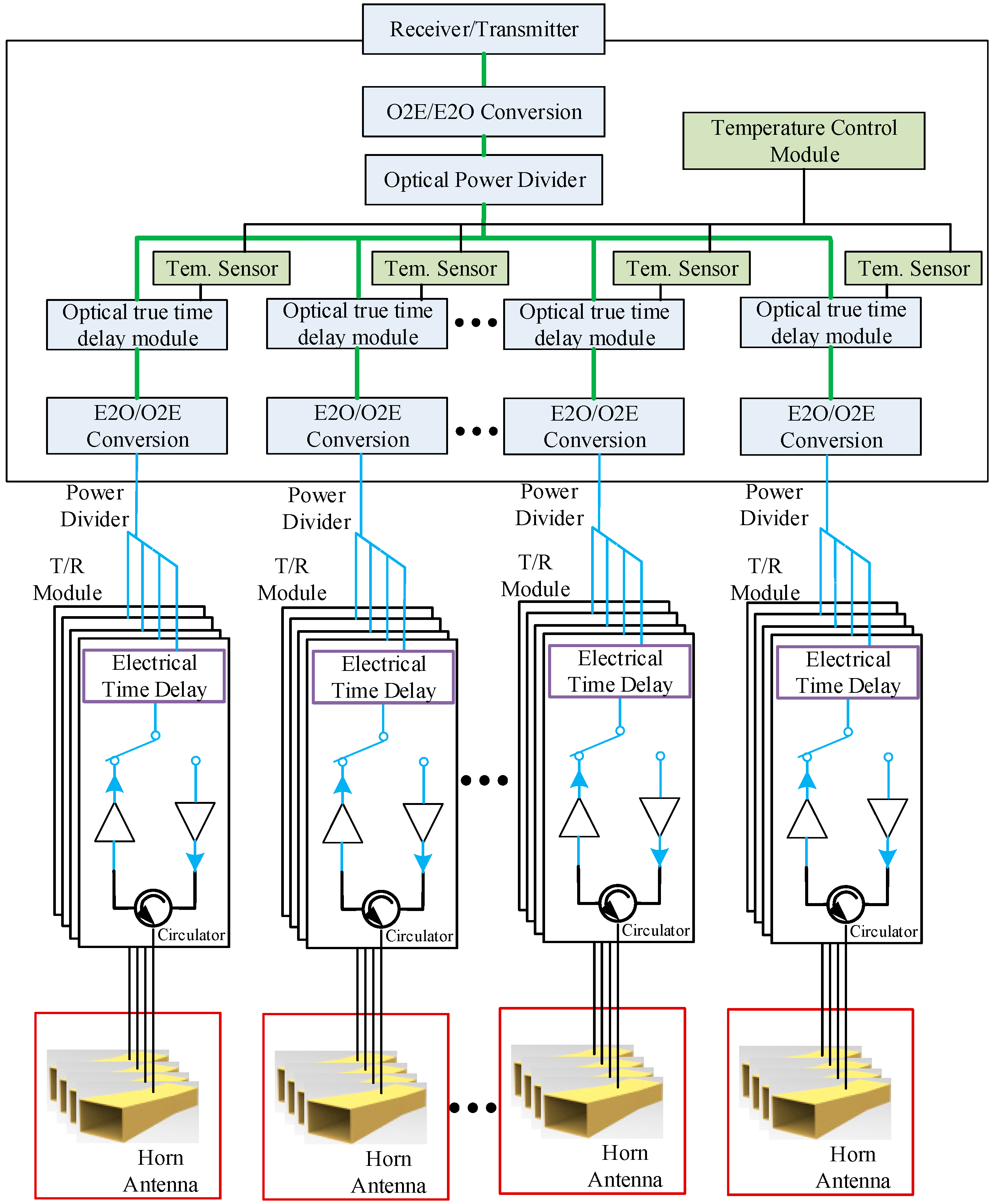
The whole phased array was composed of a passive antenna, a transmitting/receiving (T/R) module, and an optical network module, as shown in Figure 1. The T/R module consisted of a microwave amplifier that included a low-noise amplifier (LNA), power amplifier (PA), circulator, and switching mechanism, which could isolate the transmitting and receiving links, as well as an electrical time-delay module. The phase shifting of each channel was controlled by a beam controller, which is not shown in the figure. Firstly, a modular structure was adopted to divide each part according to the functional modules, and the hardware structure could also be assembled and tested independently. Finally, each part was assembled and integrated through corresponding interface relations to form the whole antenna array. The advantage of this design was that the whole antenna array was divided into many small standard modules, and each standard module was individually assembled and debugged, which reduced the complexity of the assembly and provided convenience for the testing of the physical structure of the module.
A horn antenna was chosen as the antenna element of the phased array. It received and transmitted the microwave signal from/to free space. The antennas were connected to the TR module. The TR module included a low-noise amplifier and a power amplifier; the low-noise amplifier was used to amplify the received microwave signal, and the power amplifier was responsible for amplifying the transmitted microwave signal. Taking the receiving link as an example, the microwave signal was converted into an optical signal through an electro-optical conversion module and then phase shifted through the delay line in the optical module to realize the phase difference between each unit. Multiple phase-shifted optical signals passed through the optical power divider to synthesize a single optical-band received signal, and through the photoelectric conversion module, the optical signal was converted into a microwave signal, which entered the microwave receiver for post-processing. The process in the transmitting link was similar to this, but the signal flow was different.
It is noted that in this design, we used a hybrid solution of an optical time delay plus an electronic time delay. This scheme allowed the large time delay of the optical fiber and the small electronic time delay to be taken advantage of. It was able to provide wide-angle scanning while improving the beam-pointing accuracy, which is very important in radar application scenarios.
As shown in Figure 1, each antenna was connected to an electronic time delay at the rear end, which was used to appropriately delay the reception or transmission. The signal passed through the T/R module and the power divider and then flowed into the optoelectronic/electro-optical converter module, after which it was delayed by the optical time delay. This architecture enabled two-dimensional beam scanning, but the optical delay was added after the antenna sub-array of four antennas and four T/R modules. Thus, the antenna actually performed one-dimensional beam scanning, i.e., beam scanning in the direction of the arrangement of the optical time delays.
2.1. Configuration and Mechanism of the Antenna and TR Module
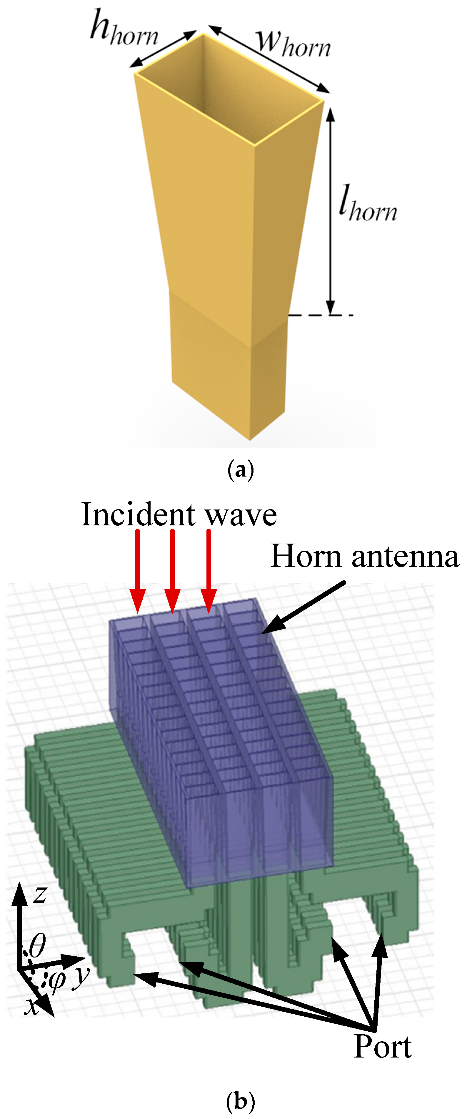
The microwave antenna included the radiation structure of the antenna array, RF feed network, and RF T/R module. In order to obtain the wideband, high-gain, and wide-beam performance, the form of a horn antenna was selected, and the structure is shown in Figure 2a. The waveguide horn antenna had the advantages of a small size, light weight, compact structure, and so on. Therefore, the waveguide horn antenna was finally selected as the element for the 16 × 4 passive antenna array in this study, and its structure is shown in Figure 2a. In order to achieve antenna performance with a scanning range of θ ≥ 30° in the band range of 12–17 GHz (azimuthal scanning), the spacing of antenna elements can be calculated with the following formulas:
where θmax is the maximum scanning angle, λmin is the highest frequency wavelength, dx is the azimuth element spacing, and dy is the element spacing in the vertical direction. According to the formula, the azimuth spacing of antenna elements should be less than 11.7 mm. In the array layout, considering the product of the antenna’s power aperture, beam width, scanning range, and other factors, the azimuth spacing of antenna elements was determined to be 10.9 mm, thus meeting the requirement of having no grating lobes in the scanning range of the system. On this basis, a brick structure was adopted, and the array is formed with basic modules to optimize 16 array elements (each of which contained 4 pitching channels) and 64 channels in total.
Because the antenna’s instantaneous bandwidth was very wide, the feed network of all channels needed to be designed with an equal length in order to ensure that the requirements of equal amplitude and phase were fulfilled. Considering the technical difficulty, producibility, and reliability, a waveguide was finally used to form the antenna RF feed network. The structure is shown in Figure 2b. The advantage of this design was its use of the precision of the structure’s processing to ensure amplitude and phase consistency between channels so as to improve performance. The requirements for cable production are very harsh, so if a cable connection was adopted, it would be difficult to ensure productivity.
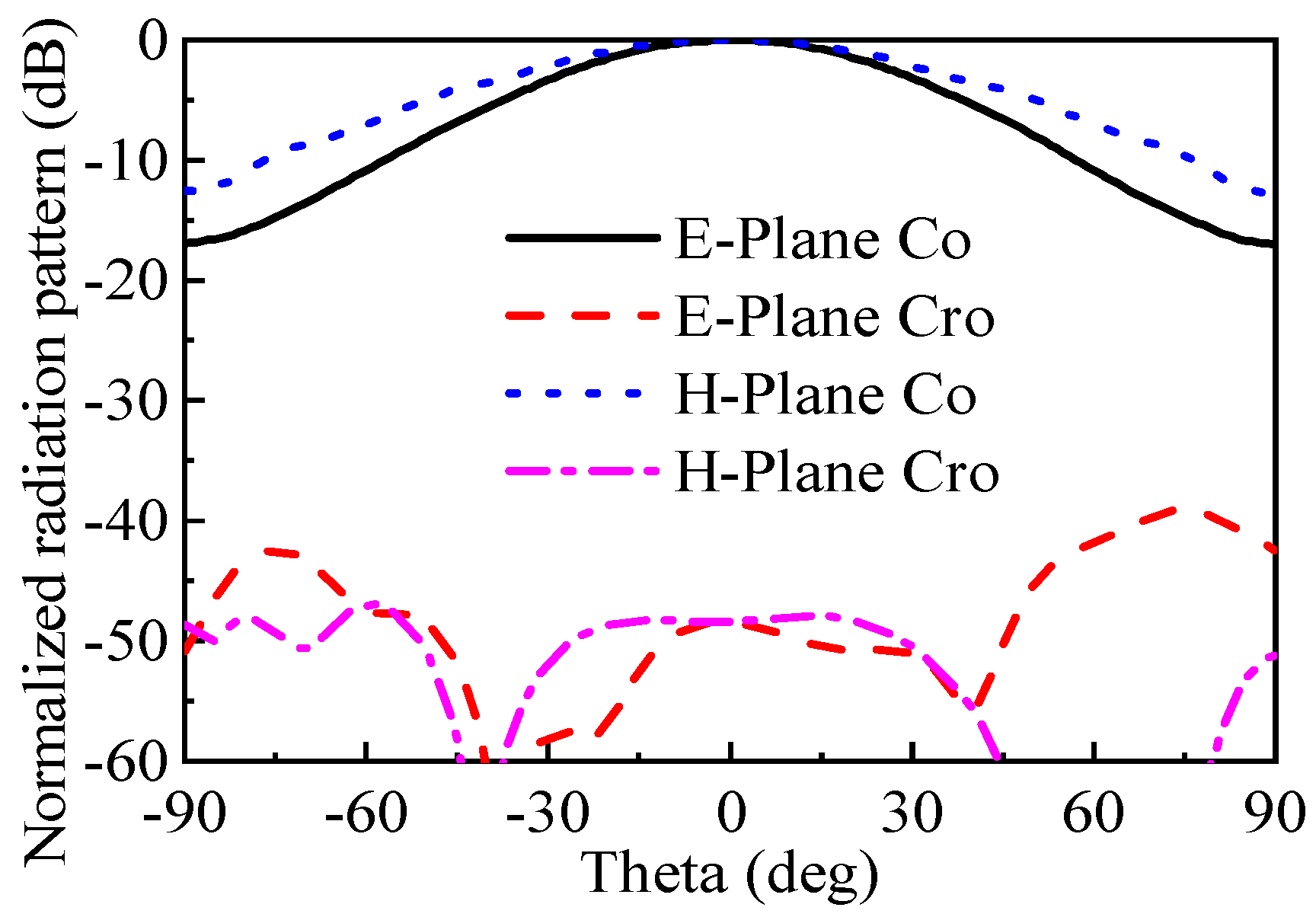
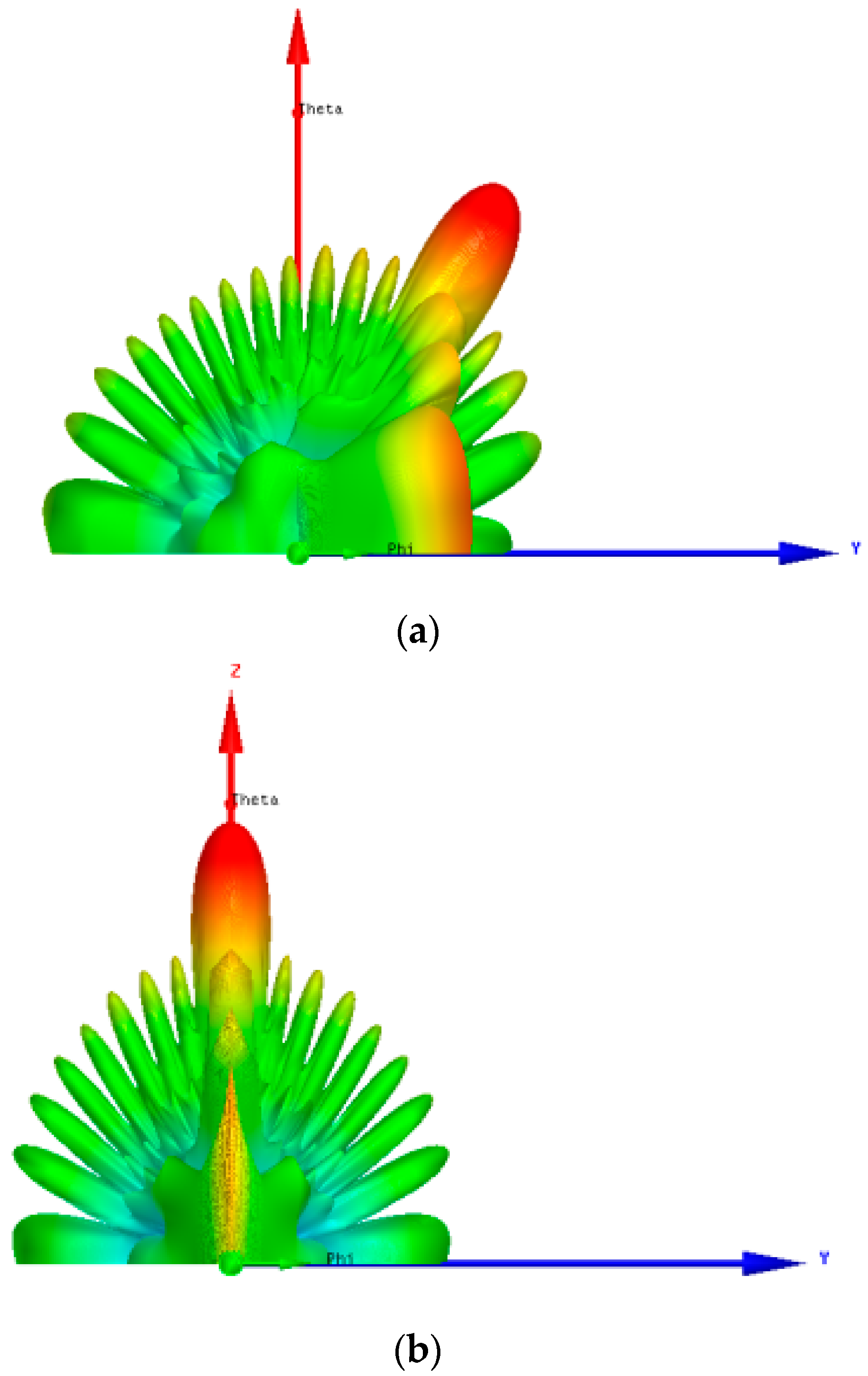
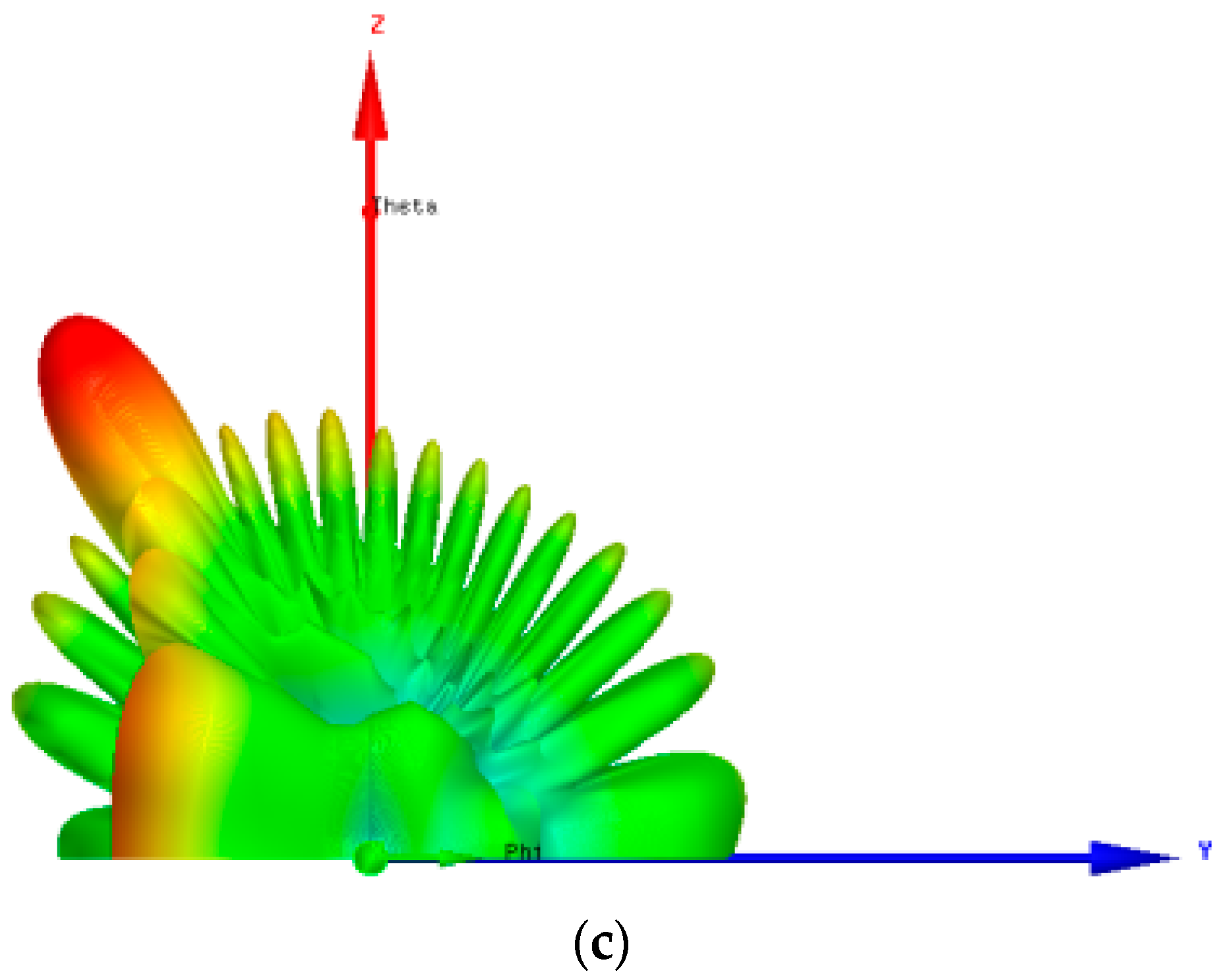
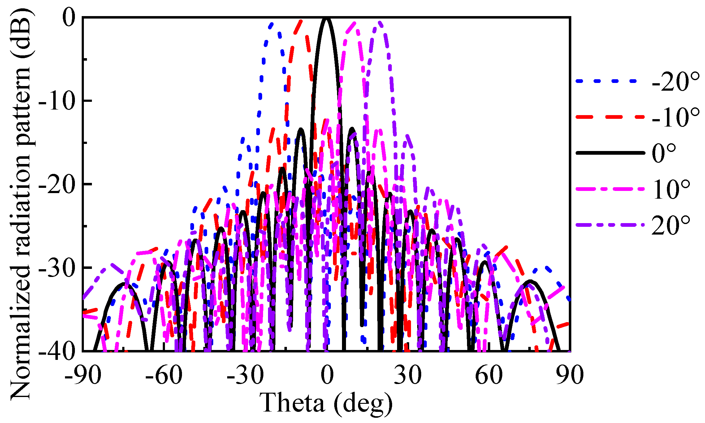
Figure 3 shows the simulated radiation pattern of the horn element, while the simulated 3D radiation patterns at different scanning angles of the antenna array are shown in Figure 4. As shown in the figure, the horn antenna had a wide beam and a low level of cross-polarization. The antenna was able to scan at the desired angle. Figure 5 shows the simulated 2D E-plane radiation pattern of the antenna at different scanning angles at 14.5 GHz. In the figure, one can see that the antenna was able to maintain a low sidelobe when scanning at 20°. It is noted that in the simulation, the feeding amplitude was set as constant.
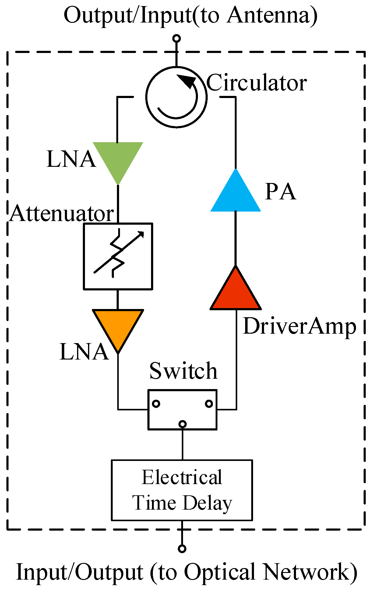
Figure 6 shows a schematic diagram of a single TR channel. Specifically, the TR channel contained a circulator, a switch, an electrical time-delay module, an amplifier, and an attenuator for the control of the power amplifier’s amplitude. The amplifier for the receiving link contained two low-noise amplifiers (LNAs) for the amplification of small signals, while the amplifier for the transmitting link contained a power amplifier (PA) and a pre-amplifier for the PA. It is noted that an LNA is a kind of power amplifier with quite low-noise features. A drive amplifier was used to amplify a microwave signal at the primary level, after which the signal entered a power amplifier for the high-power signal output. The use of a circulator and switch ensured that the receiving and transmitting links could work simultaneously.
Usually, for true time-delay devices, optical time-delay devices have the advantages of a large time delay and low insertion loss, and they can usually meet the beam-scanning requirements of phased arrays with large angles. However, the time-delay step of optical time-delay devices is usually large, which makes it impossible to achieve high-precision beam pointing. In this design, in addition to the optical time-delay device, we added an electrical time-delay device inside the T/R component. An electronic time-delay device (NC12164C-618) from the 13th Research Institute of China Electronics Technology Corporation (CETC) was chosen as the electronic time-delay device. This device is an electronic time-delay device with six-bit quantization accuracy, a minimum delay of 1.3 ps, a maximum delay of 82 ps, and a delay step of 1.3 ps.
2.2. Configuration and Mechanism of the Optical Network Module
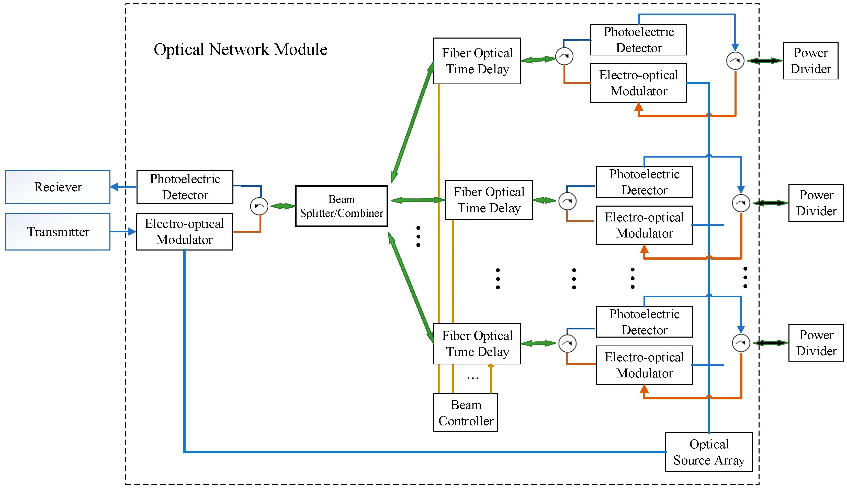
A diagram of the optical network module is shown in Figure 7. The whole beam-control unit consisted of seven parts, including an electro-optical modulation module, optical circulator, optical delay line module, beam splitter/combiner, photoelectric detector, and optical source. To control the temperature of the fiber, we added a temperature control module to keep it stable. This allowed the requirement of high dynamic operating temperatures to be met.
When the beam-control unit worked in transmission mode, the signal sent by the transmitter was firstly converted into an optical signal using the electro-optical modulator and then divided into several channels by the beam splitter. After that, the signal entered the optical-fiber delay line to obtain the time delay set by the wave controller and, finally, was converted into an electrical signal. When working in the receiving mode, the signal received by the antenna unit was amplified by the T/R component and converted into an optical signal using the electro-optical modulator; then, it entered the optical-fiber delay line through electro-optical conversion to obtain the time delay set by the wave controller, and one channel was synthesized by the beam combiner. After photoelectric conversion, it became a microwave signal and entered the radar receiver. In general, the optical transmitter used electro-optic modulation technology to load the microwave signal onto a light wave, and the optical receiver used a photodetector to recover the microwave signal contained in a light wave and synthesize the output. The OE–EO conversion loss was about 20 dB, and this loss reduced the efficiency of the system to a certain extent. In order to improve the efficiency of the system, we added an optical amplifier to reduce the OE–EO conversion loss.
An optical-fiber delay line was adopted in the delay module, as it was able to realize different real delays in the propagation. The modulation of radar microwave signals into light waves and the use of optical fiber to transmit radar signals have obvious advantages because the transmission loss of optical fiber is much lower than that of coaxial cables and waveguide transmission over the whole radar frequency range. Moreover, the signal loss at all frequencies is the same, which is very beneficial for the remote control of radar systems and the transmission and distribution of radar signals.
In this design, the phased array required a maximum beam scanning angle of 30 degrees. According to the antenna array principle, the maximum delay required by the phased array antenna unit can be calculated with the following equation:
where d denotes the antenna element spacing, which was 10.9 mm here, and θ is the maximum scanning angle of the antenna, which was set to 30 degrees in this antenna design. n is the number of antenna units, which was 16 here, and c is the speed of light in free space. The maximum delay required by the antenna was 272.5 ps.
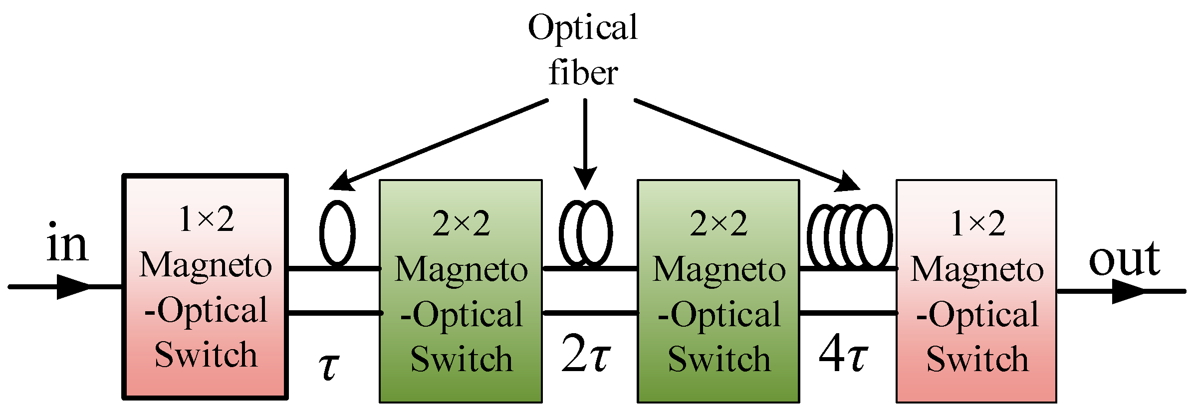
To achieve the maximum delay and delay step requirements, the designed beamforming network needed to have a six-bit phase-shifting accuracy, and in order to achieve higher phase-shifting accuracy and lower system complexity, we chose a composite optical beamforming network, which consisted of a three-bit optical switch array and a six-bit electrical delay line to form a series-connected time-delay network. The optical delay line is shown in Figure 8. It consisted of two 2 × 2 magneto-optical switches and two 1 × 2 magneto-optical switches; the light was input into the 1 × 2 magneto-optical switches, passed through two 2 × 2 magneto-optical switches in sequence, and, finally, passed through the output of the 1 × 2 magneto-optical switches. The lengths of the two optical fibers that were output from each level of the magneto-optical switches differed by a factor of 2n.
The phase shift accuracy of the beamforming network was directly affected by the malignancy of the optical fiber due to the use of fiber as a delay device. Usually, the characteristics of a fiber change significantly at different temperatures, which, in turn, affects the phase-shift characteristics of optical signals, resulting in a large phase-shift error and a significant degradation of the scanning performance of the antenna. To improve the stability of the phased array, a temperature control module was introduced to monitor the temperature of the optical network module in real time, and it was used to accurately regulate the temperature so that the optical network module could have better temperature stability. Table 1 shows the delay time values of the optical delay network at different ambient temperatures after adopting temperature stabilization. Here, we chose four channels for testing with a temperature range of 0°–30°. The designed delay value was 65 ps. In the table, it can be seen that with temperature stabilization, the optical network module was able to achieve stable phase-shift values with an error of less than 2 ps at different ambient temperatures.
3. Simulated and Measured Results
To verify the design, a prototype of the presented antenna system was fabricated and measured, as illustrated in Figure 9. Each part was separately designed and installed; then the whole assembly was made. The external interface of the product used connectors for simple and convenient interconnection, and the internal interface used cables and welding for electrical interconnection.
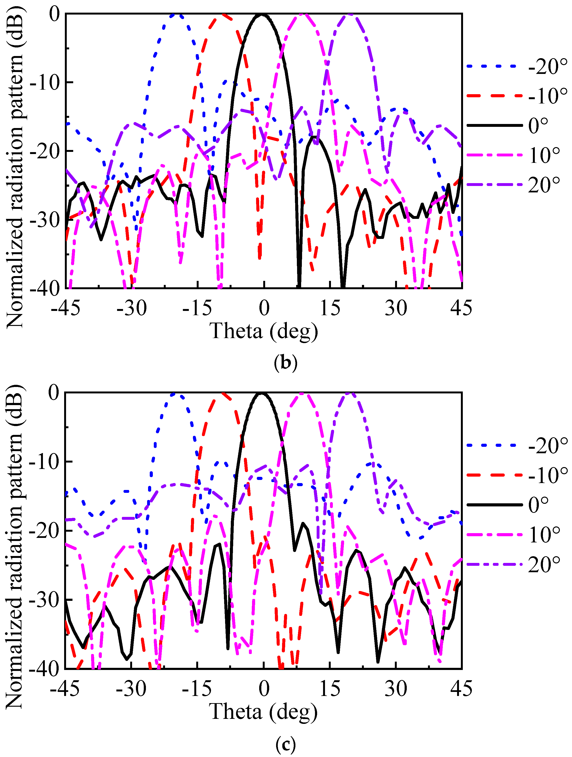
When conducting measurements, to realize the low-sidelobe requirement for the array antenna, the Taylor amplitude weighting was used to design the feed amplitude. Figure 10 shows the measured radiation patterns of the presented antenna system when the array scanned at different angles along the E-plane at 12 GHz, 14.5 GHz, and 17 GHz. As can be seen in the figures, when the antenna array scanned at an angle of 0°, its sidelobe level was higher than 18 dB at all of the frequencies. When the antenna array reached a scanning angle of 30°, the sidelobe level was higher than 18 dB at 12 GHz and 12 dB at 14.5 and 17 GHz. From the results, one can see that over a wide operating bandwidth, the beam-scanning angle of the antenna was kept almost constant.
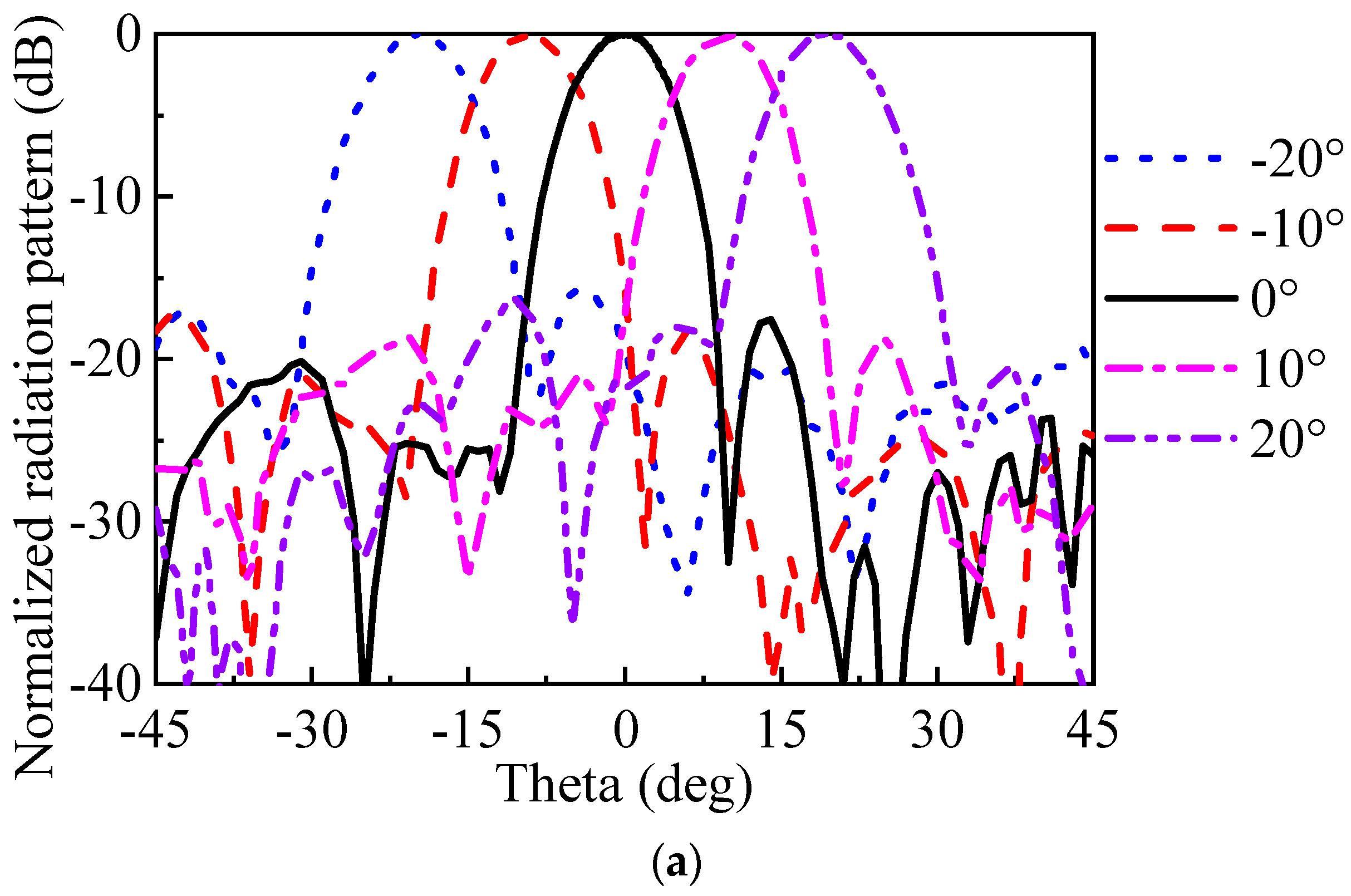
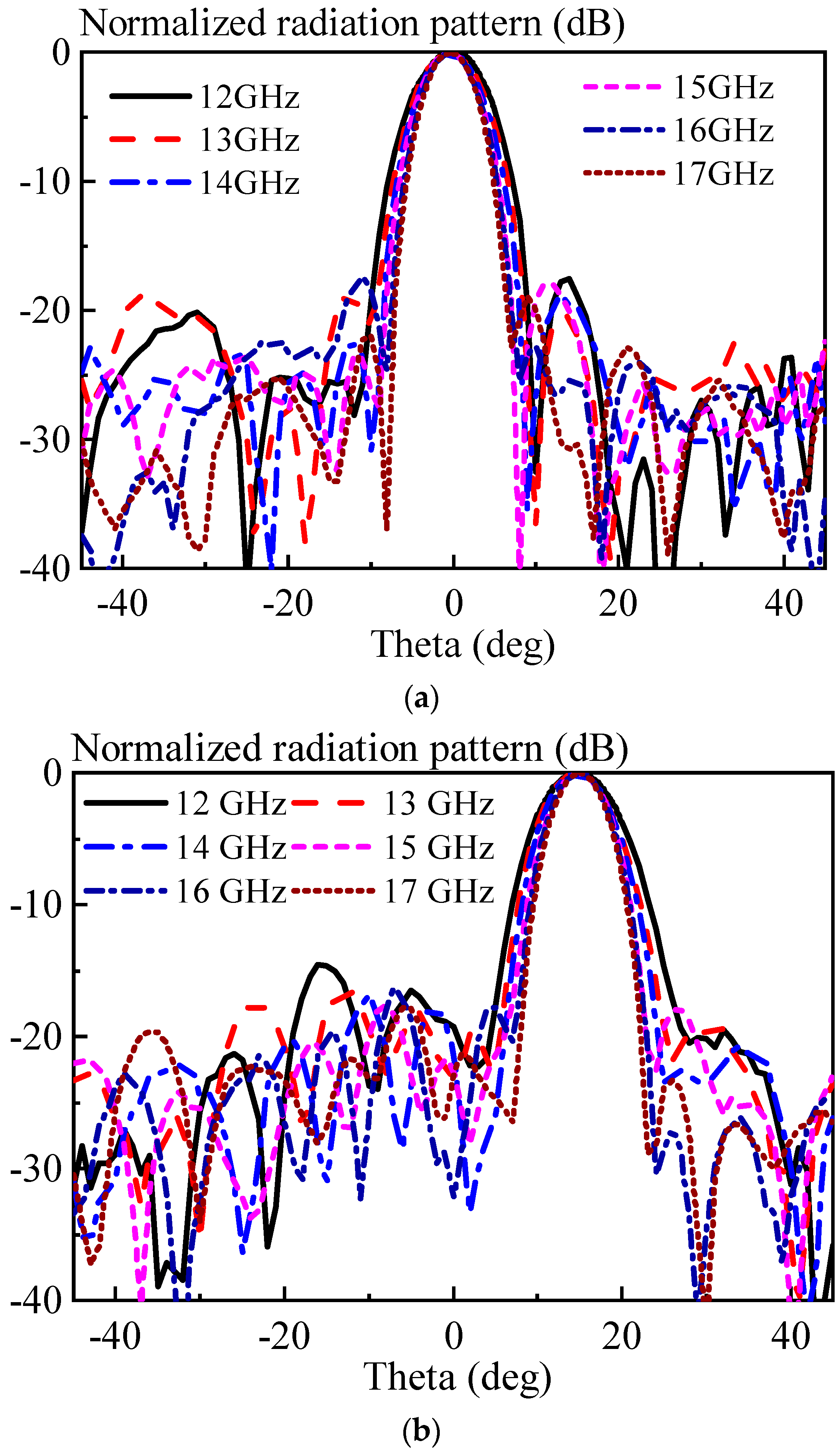
To verify the beam-scanning characteristics of the proposed microwave photonics over a wide range of bandwidths, we tested the beam characteristics of the antenna in the frequency range of 12–15 GHz, where the wave-control codebook used for the phased array was consistent. Figure 11 shows a two-dimensional orientation diagram of the antenna when the scanning angles of the antenna were 0 and 15 degrees. In the figure, it can be seen that the beam pointing of the antenna had almost no offset at different frequencies, and there were no beam-squint phenomena, which proved the instantaneous broadband characteristics of the antenna.
To emphasize the advantages of this phased array design, we compared the performance in terms of the operating frequency, bandwidth, beam-scanning angle, phase quantization, and temperature control of existing work and the work proposed here. The results of this comparison are summarized in Table 2. In the table, it can be seen that in most of the previously published literature, temperature control was not included. The beam-scanning angle and bandwidth of the antenna were basically the same as those of other antennas, while our antenna had the highest phase quantization, namely, nine bits. This high phase quantization was able to ensure beam-pointing accuracy and is quite important for large-scale antenna arrays in radar applications.
4. Conclusions
A one-dimensional active broadband phased array antenna that works in the Ku band was proposed to achieve a large instantaneous bandwidth. The antenna is mainly composed of a broadband phased array antenna and an optical network module. The optical network module and broadband phased array antenna were introduced in detail in this study. The experimental results showed that the optical phased array antenna was able to scan ±20° from 12 GHz to 17 GHz, and the beam pointing did not appear to be offset. The antenna had features that allowed it to widely scan with a large bandwidth.
Author Contributions
Conceptualization, Y.L., J.R. and R.L.; Methodology, T.Y.; Software, Y.L. and T.Y.; Validation, Y.L.; Data curation, J.R.; Writing—original draft, Y.L. and T.Y.; Writing—review & editing, J.R.; Project administration, Z.Z.; Funding acquisition, Z.Z. All authors have read and agreed to the published version of the manuscript.
Funding
This research received no external funding.
Data Availability Statement
Data is contained within the article.
Conflicts of Interest
The authors declare no conflicts of interest.
References
- Parker, D.; Zimmermann, D.C. Phased arrays—Part 1: Theory and architectures. IEEE Trans. Microw. Theory Tech. 2002, 50, 678–687. [Google Scholar] [CrossRef]
- Parker, D.; Zimmermann, D.C. Phased arrays-part II: Implementations, applications, and future trends. IEEE Trans. Microw. Theory Tech. 2002, 50, 688–698. [Google Scholar] [CrossRef]
- Hansen, R.C. Phased Array Antennas; John Wiley & Sons: Hoboken, NJ, USA, 2009. [Google Scholar]
- Fenn, A.J.; Hurst, P.T. Ultrawideband Phased Array Antenna Technology for Sensing and Communications Systems; MIT Press: Cambridge, MA, USA, 2015. [Google Scholar]
- Yang, G.; Li, J.; Wei, D.; Xu, R. Study on wide-angle scanning linear phased array antenna. IEEE Trans. Antennas Propag. 2018, 66, 450–455. [Google Scholar] [CrossRef]
- Han, G.; Du, B.; Wu, W.; Yang, B. A novel hybrid phased array antenna for satellite communication on-the-move in Ku-band. IEEE Trans. Antennas Propag. 2015, 63, 1375–1383. [Google Scholar] [CrossRef]
- Hashemi, H.; Xiang, G.; Komijani, A.; Hajimiri, A. A 24-Ghz Sige phased-array receiver-LO phase-shifting approach. IEEE Trans. Microw. Theory Tech. 2005, 53, 614–626. [Google Scholar] [CrossRef]
- Zihir, S.; Gurbuz, O.D.; Kar-Roy, A.; Raman, S.; Rebeiz, G.M. 60-ghz 64- and 256-elements wafer-scale phased-array transmitters using full-reticle and subreticle stitching techniques. IEEE Trans. Microw. Theory Tech. 2016, 64, 4701–4719. [Google Scholar] [CrossRef]
- Kibaroglu, K.; Sayginer, M.; Phelps, T.; Rebeiz, G.M. A 64-element 28-ghz phased-array transceiver with 52-dBm eirp and 8–12-Gb/s 5G link at 300 meters without any calibration. IEEE Trans. Microw. Theory Tech. 2018, 66, 5796–5811. [Google Scholar] [CrossRef]
- Ku, B.H.; Schmalenberg, P.; Inac, O.; Gurbuz, O.D.; Lee, J.S.; Shiozaki, K.; Rebeiz, G.M. A 77–81-ghz 16-element phased-array receiver ±50º beam scanning for advanced automotive radars. IEEE Trans. Microw. Theory Tech. 2014, 62, 2823–2832. [Google Scholar] [CrossRef]
- Zhang, H.; Yang, S.; Chen, Y.; Guo, J.; Nie, Z. Wideband dual-polarized linear array of tightly coupled elements. IEEE Trans. Antennas Propag. 2018, 66, 476–480. [Google Scholar] [CrossRef]
- Zhang, H.; Yang, S.; Xiao, S.; Chen, Y.; Qu, S. Low-profile, lightweight, ultra-wideband tightly coupled dipole arrays loaded with split rings. IEEE Trans. Antennas Propag. 2019, 67, 4257–4262. [Google Scholar] [CrossRef]
- Zhang, L.; Gao, S.; Luo, Q.; Li, W.; He, Y.; Li, Q. A wideband circularly polarized tightly coupled array. IEEE Trans. Antennas Propag. 2018, 66, 6382–6387. [Google Scholar] [CrossRef]
- Wu, W.; Yan, Y.; Wang, S.; Ma, Y.; Yuan, N. An ultrathin Low-profile tightly coupled dipole array fed by compact zigzagging baluns. Electronics 2023, 12, 2752. [Google Scholar] [CrossRef]
- Li, W.; Qiu, T.; Wang, J.; Zheng, L.; Jing, Y.; Jia, Y.; Wang, H.; Han, Y.; Qu, S. Programmable coding metasurface reflector for reconfigurable multibeam antenna application. IEEE Trans. Antennas Propag. 2021, 69, 296–301. [Google Scholar] [CrossRef]
- Zhang, N.; Chen, K.; Zhao, J.; Hu, Q.; Tang, K.; Zhao, J.; Jiang, T.; Feng, Y. A dual-polarized reconfigurable reflectarray antenna based on dual-channel programmable metasurface. IEEE Trans. Antennas Propag. 2022, 70, 7403–7412. [Google Scholar] [CrossRef]
- Li, P.; Ren, J.; Chen, Y.; Ren, X.; Xu, K.D.; Yin, Y.Z.; Shen, M. Design of low-cost single-layer 2-bit reflective programmable metasurface based on folded ground. IEEE Trans. Microw. Theory Tech. 2023, 71, 3455–3465. [Google Scholar] [CrossRef]
- Lee, J.-G.; Lee, J.-H. Low-profile high-efficiency transmitarray antenna for beamforming applications. Electronics 2023, 12, 3178. [Google Scholar] [CrossRef]
- Teodorani, L.; Vernì, F.; Giordanengo, G.; Gaffoglio, R.; Vecchi, G. experimental demonstration of beam scanning of dual-metasurface antenna. Electronics 2023, 12, 1833. [Google Scholar] [CrossRef]
- Esteban Eraso, U.; Sánchez-Azqueta, C.; Aldea, C.; Celma, S. A 19.5 ghz 5-bit digitally programmable phase shifter for active antenna arrays. Electronics 2023, 12, 2862. [Google Scholar] [CrossRef]
- Bai, Y.Y.; Xiao, S.; Liu, C.; Wang, B.Z. A hybrid IWO/PSO algorithm for pattern synthesis of conformal phased arrays. IEEE Trans. Antennas Propag. 2013, 61, 2328–2332. [Google Scholar] [CrossRef]
- Bray, M.G.; Werner, D.H.; Boeringer, D.W.; Machuga, D.W. Optimization of thinned aperiodic linear phased arrays using genetic algorithms to reduce grating lobes during scanning. IEEE Trans. Antennas Propag. 2002, 50, 1732–1742. [Google Scholar] [CrossRef]
- Villegas, F.J. Parallel genetic-algorithm optimization of shaped beam coverage areas using planar 2-D phased arrays. IEEE Trans. Antennas Propag. 2007, 55, 1745–1753. [Google Scholar] [CrossRef]
- Boeringer, D.W.; Werner, D.H. Particle swarm optimization versus genetic algorithms for phased array synthesis. IEEE Trans. Antennas Propag. 2004, 52, 771–779. [Google Scholar] [CrossRef]
- Munson, R. Conformal microstrip antennas and microstrip phased arrays. IEEE Trans. Antennas Propag. 1974, 22, 74–78. [Google Scholar] [CrossRef]
- Daly, M.P.; Bernhard, J.T. Directional modulation technique for phased arrays. IEEE Trans. Antennas Propag. 2009, 57, 2633–2640. [Google Scholar] [CrossRef]
- Valavan, S.E.; Tran, D.; Yarovoy, A.G.; Roederer, A.G. Planar dual-band wide-scan phased array in X-band. IEEE Trans. Antennas Propag. 2014, 62, 5370–5375. [Google Scholar] [CrossRef]
- Wang, R.; Wang, B.Z.; Ding, X.; Yang, X.S. Planar phased array with Wide-angle scanning performance based on image theory. IEEE Trans. Antennas Propag. 2015, 63, 3908–3917. [Google Scholar] [CrossRef]
- Liu, C.M.; Xiao, S.Q.; Tu, H.L.; Ding, Z. Wide-angle scanning low profile phased array antenna based on a novel magnetic dipole. IEEE Trans. Antennas Propag. 2017, 65, 1151–1162. [Google Scholar] [CrossRef]
- Bai, Y.Y.; Xiao, S.; Tang, M.C.; Ding, Z.F.; Wang, B.Z. Wide-angle scanning phased array with pattern reconfigurable elements. IEEE Trans. Antennas Propag. 2011, 59, 4071–4076. [Google Scholar] [CrossRef]
- Moon, S.M.; Yun, S.; Yom, I.B.; Lee, H.L. Phased array shaped-beam satellite antenna with boosted-beam control. IEEE Trans. Antennas Propag. 2019, 67, 7633–7636. [Google Scholar] [CrossRef]
- Ding, Y.R.; Cheng, Y.J.; Sun, J.X.; Wang, L.; Li, T.J. Dual-band shared-aperture two-dimensional phased array antenna with wide bandwidth of 25.0% and 11.4% at ku- and ka-band. IEEE Trans. Antennas Propag. 2022, 70, 7468–7477. [Google Scholar] [CrossRef]
- Pan, S.; Zhang, Y. Microwave photonic radars. J. Light. Technol. 2020, 38, 5450–5484. [Google Scholar] [CrossRef]
- Pan, S.; Ye, X.; Zhang, Y.; Zhang, F. Microwave photonic array radars. IEEE J. Microw. 2021, 1, 176–190. [Google Scholar] [CrossRef]
- Attygalle, M.; Stepanov, D. Photonic technique for phase control of microwave to terahertz signals. IEEE Trans. Microw. Theory Tech. 2014, 62, 1381–1386. [Google Scholar] [CrossRef]
- Tang, Z.; Pan, S. A reconfigurable photonic microwave mixer using a 90° optical hybrid. IEEE Trans. Microw. Theory Tech. 2016, 64, 3017–3025. [Google Scholar] [CrossRef]
- Tulchinsky, D.A.; Matthews, P.J. Ultrawide-band fiber-optic control of a millimeter-wave transmit beamformer. IEEE Trans. Microw. Theory Tech. 2001, 49, 1248–1253. [Google Scholar] [CrossRef]
- Yu, Y.; Shang, Q.; An, S.; Zhang, Y.; Su, Y.; Yao, J. Tunable silicon photonic RF phase shifter with low RF power variation based on constructive interference of an add-drop ring resonator. IEEE Photonics J. 2018, 10, 1–8. [Google Scholar] [CrossRef]
- Zhang, Y.; Pan, S. Broadband microwave signal processing enabled by polarization-based photonic microwave phase shifters. IEEE J. Quantum Electron. 2018, 54, 1–12. [Google Scholar] [CrossRef]
- Zhou, P.; Zhang, F.; Pan, S. Generation of linear frequency-modulated waveforms by a frequency-sweeping optoelectronic oscillator. J. Light. Technol. 2018, 36, 3927–3934. [Google Scholar] [CrossRef]
- Wang, M.; Yao, J. Tunable 360° photonic radio-frequency phase shifter based on polarization modulation and all-optical differentiation. J. Light. Technol. 2013, 31, 2584–2589. [Google Scholar] [CrossRef]
- Zhang, X.; Hosseini, A.; Lin, X.; Subbaraman, H.; Chen, R.T. Polymer-based hybrid-integrated photonic devices for silicon on-chip modulation and board-level optical interconnects. IEEE J. Sel. Top. Quantum Electron. 2013, 19, 196–210. [Google Scholar] [CrossRef]
- Bui, L.A.; Mitchell, A.; Ghorbani, K.; Chio, T.-H.; Mansoori, S.; Lopez, E.R. Wide-band photonically phased array antenna using vector sum phase shifting approach. IEEE Trans. Antennas Propag. 2005, 53, 3589–3596. [Google Scholar] [CrossRef]
- McKenna, T.P.; Nanzer, J.A.; Clark, T.R. Photonic beamsteering of a millimeter-wave array with 10-Gb/s data transmission. IEEE Photonics Technol. Lett. 2014, 26, 1407–1410. [Google Scholar] [CrossRef]
- Meijerink, A.; Roeloffzen, C.G.H.; Meijerink, R.; Zhuang, L.; Marpaung, D.A.I.; Bentum, M.J.; Burla, M.; Verpoorte, J.; Jorna, P.; Hulzinga, A.; et al. Novel ring resonator-based integrated photonic beamformer for broadband phased array receive antennas—Part I: Design and performance analysis. J. Light. Technol. 2010, 28, 3–18. [Google Scholar] [CrossRef]
- Zhuang, L.; Roeloffzen, C.G.H.; Meijerink, A.; Burla, M.; Marpaung, D.A.I.; Leinse, A.; Hoekman, M.; Heideman, R.G.; Etten, W.V. Novel ring resonator-based integrated photonic beamformer for broadband phased array receive antennas—Part II: Experimental prototype. J. Light. Technol. 2010, 28, 19–31. [Google Scholar] [CrossRef]
- Tsokos, C.; Andrianopoulos, E.; Raptakis, A.; Lyras, N.K.; Gounaridis, L.; Groumas, P.; Timens, R.B.; Visscher, I.; Grootjans, R.; Wefers, L.S.; et al. True time delay optical beamforming network based on hybrid inp-silicon nitride integration. J. Light. Technol. 2021, 39, 5845–5854. [Google Scholar] [CrossRef]
- Zheng, P.; Wang, C.; Xu, X.; Li, J.; Lin, D.; Hu, G.; Zhang, R.; Yun, B.; Cui, Y. A seven bit silicon optical true time delay line for ka-band phased array antenna. IEEE Photonics J. 2019, 11, 1–9. [Google Scholar] [CrossRef]
- Paula, I.L.d.; Bogaert, L.; Caytan, O.; Kerrebrouck, J.V.; Moerman, A.; Muneeb, M.; Brande, Q.V.d.; Torfs, G.; Bauwelinck, J.; Rogier, H.; et al. Air-filled SIW remote antenna unit with true time delay optical beamforming for mmWave-Over-fiber systems. J. Light. Technol. 2022, 40, 6961–6975. [Google Scholar] [CrossRef]
- Carey, V.A.; Konkol, M.R.; Shi, S.; Mercante, A.J.; Shreve, K.; Wright, A.A.; Schuetz, C.A.; Prather, D.W. Millimeter wave photonic tightly coupled array. IEEE Trans. Antennas Propag. 2021, 69, 4488–4503. [Google Scholar] [CrossRef]
- Ross, D.D.; Konkol, M.R.; Shi, S.; Harrity, C.E.; Wright, A.A.; Schuetz, C.A.; Prather, D.W. Low-profile high-power optically addressed phased array antenna. J. Light. Technol. 2017, 35, 3894–3900. [Google Scholar] [CrossRef]
- Shi, S.; Bai, J.; Schneider, G.J.; Zhang, Y.; Nelson, R.; Wilson, J.; Schuetz, C.; Grund, D.W.; Prather, D.W. Conformal wideband optically addressed transmitting phased array with photonic receiver. J. Light. Technol. 2014, 32, 3468–3477. [Google Scholar] [CrossRef]
Figure 1.
A schematic diagram of the microwave-photonics-based broadband phased array.

Figure 2.
Structure of the presented antenna. (a) Antenna element. Dimensions: whorn = 10.9 mm, hhorn = 5.5 mm, lhorn = 25 mm. (b) Antenna array with the feed network.
Figure 2.
Structure of the presented antenna. (a) Antenna element. Dimensions: whorn = 10.9 mm, hhorn = 5.5 mm, lhorn = 25 mm. (b) Antenna array with the feed network.

Figure 3.
The normalized radiation pattern of the horn antenna element. Co and Cro indicate that the polarization was the same as the antenna’s polarization (coplanar) or perpendicular to the antenna’s polarization (cross).
Figure 3.
The normalized radiation pattern of the horn antenna element. Co and Cro indicate that the polarization was the same as the antenna’s polarization (coplanar) or perpendicular to the antenna’s polarization (cross).

Figure 4.
Simulated 3D radiation patterns of the phased array at different beam-scanning angles. The red means the maximum value and the blue means the minimum value. (a) Scanning angle: 30°. (b) Scanning angle: 0°. (c) Scanning angle: −30°.
Figure 4.
Simulated 3D radiation patterns of the phased array at different beam-scanning angles. The red means the maximum value and the blue means the minimum value. (a) Scanning angle: 30°. (b) Scanning angle: 0°. (c) Scanning angle: −30°.


Figure 5.
The realized gain of the presented antenna system in simulations and measurements.

Figure 6.
A schematic diagram of a single TR channel.

Figure 7.
A diagram of the optical network module.

Figure 8.
A diagram of the 3-bit optical beamforming network.

Figure 9.
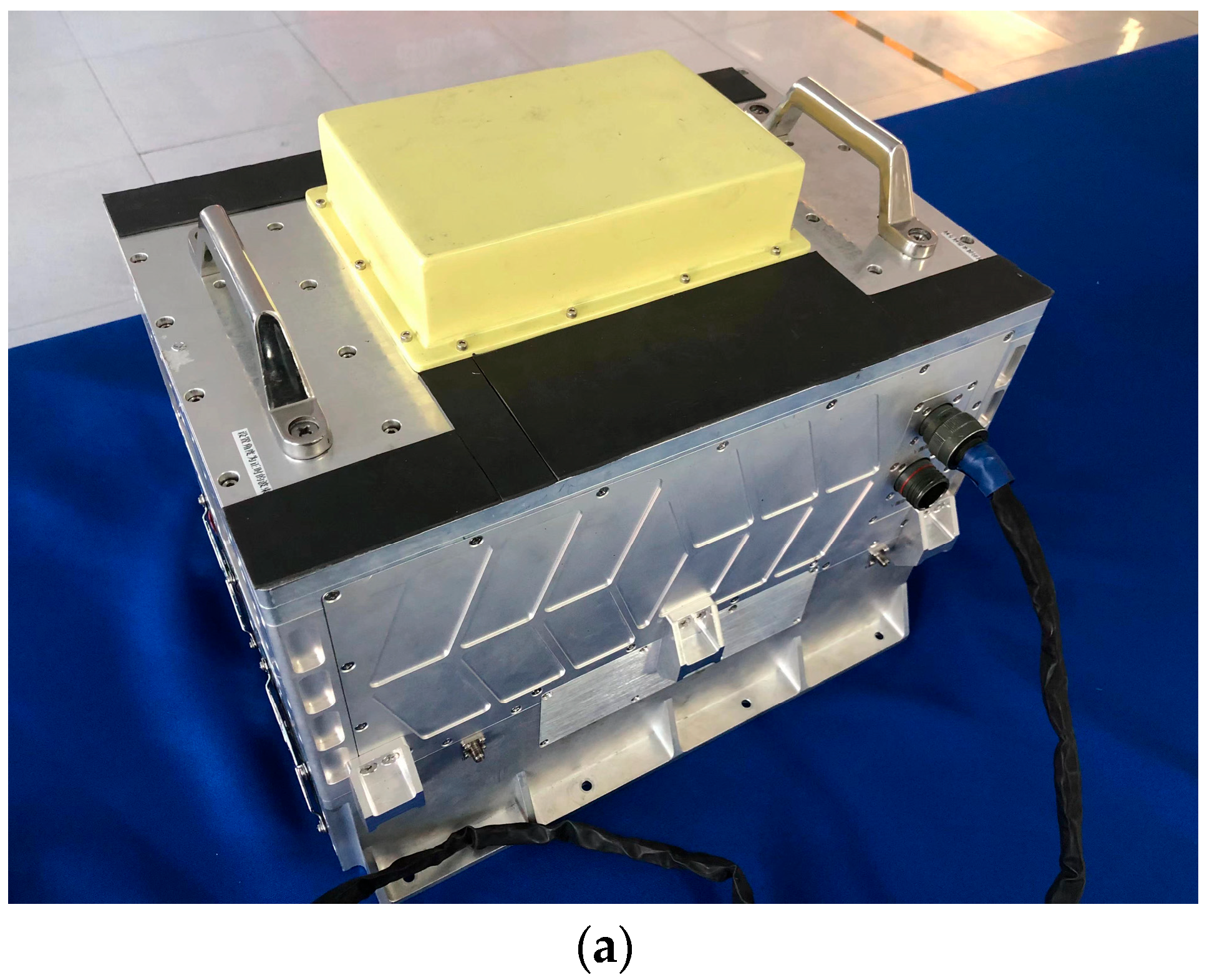
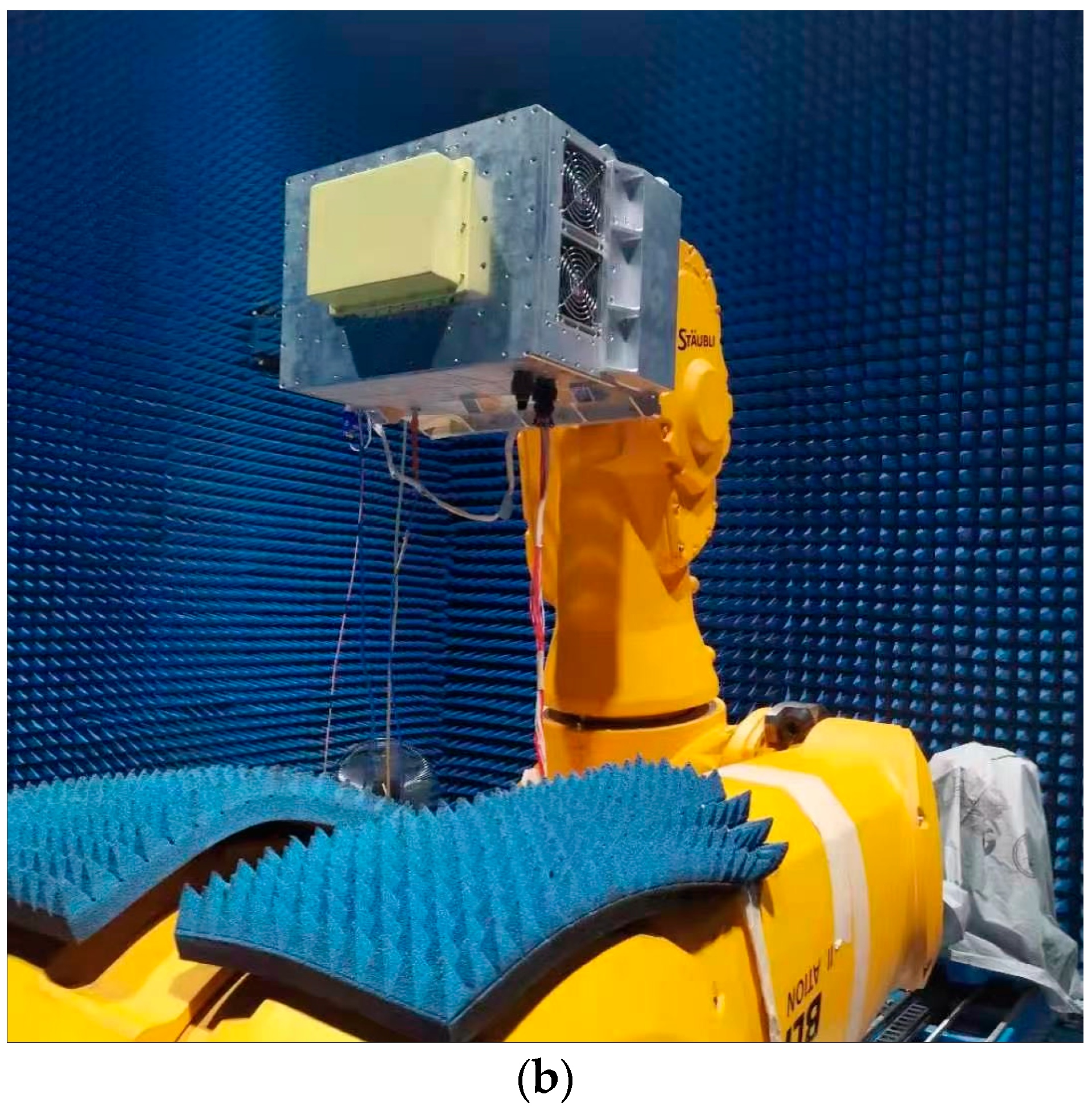
(a) A photo of the prototype of the proposed microwave-optics-based phased array. (b) The measurement setup of the antenna in a microwave chamber.
Figure 9.
(a) A photo of the prototype of the proposed microwave-optics-based phased array. (b) The measurement setup of the antenna in a microwave chamber.


Figure 10.
Measured antenna radiation patterns of the phased array (a) at 12 GHz, (b) 14.5 GHz, and (c) 17 GHz.
Figure 10.
Measured antenna radiation patterns of the phased array (a) at 12 GHz, (b) 14.5 GHz, and (c) 17 GHz.


Figure 11.
Measured antenna radiation patterns of the phased array at different frequencies: (a) 0 degrees; (b) 15 degrees.
Figure 11.
Measured antenna radiation patterns of the phased array at different frequencies: (a) 0 degrees; (b) 15 degrees.


Table 1.
The time delay of the beamforming network at different temperature. (Unit: ps).
| Temperature Degree | Channel 1 | Channel 2 | Channel 3 | Channel 4 |
|---|---|---|---|---|
| −10° | 65 | 64.4 | 65.6 | 66.9 |
| 0° | 65.6 | 64.4 | 65 | 66.3 |
| 10° | 65 | 63.8 | 65.6 | 66.3 |
| 20° | 65 | 64.4 | 65.6 | 66.3 |
| 30° | 65 | 65 | 65.6 | 66.9 |
Table 2.
Comparison between the presented antenna and other existing phased arrays.
| Ref. | Operating Band (GHz) | BW (%) | Scanning Angle | No. of Elements | Antenna Type | Temperature Control | PQ |
|---|---|---|---|---|---|---|---|
| [43] | 10–14 | 33.3 | ±30° | 16 (4 × 4) | Vivaldi antenna | No | NM |
| [44] | 85–91 | 6.8 | ±35° | NM | NM | No | 4 bit |
| [51] | 6–17 | 95.6 | ±30° | 8 (1 × 8) | Dipole antenna | No | NM |
| [52] | 34–38 | 11.1 | ±40° | 16 (4 × 4) | Patch antenna | No | NM |
| This work | 12–17 | 34.3 | ±30° | 16 (1 × 16) | Horn antenna | Yes | 9 bit |
Disclaimer/Publisher’s Note: The statements, opinions and data contained in all publications are solely those of the individual author(s) and contributor(s) and not of MDPI and/or the editor(s). MDPI and/or the editor(s) disclaim responsibility for any injury to people or property resulting from any ideas, methods, instructions or products referred to in the content. |
© 2024 by the authors. Licensee MDPI, Basel, Switzerland. This article is an open access article distributed under the terms and conditions of the Creative Commons Attribution (CC BY) license (https://creativecommons.org/licenses/by/4.0/).
Share and Cite
MDPI and ACS Style
Luan, Y.; Yang, T.; Ren, J.; Li, R.; Zhang, Z. Broadband Beam-Scanning Phased Array Based on Microwave Photonics. Electronics 2024, 13, 1278. https://0-doi-org.brum.beds.ac.uk/10.3390/electronics13071278
AMA Style
Luan Y, Yang T, Ren J, Li R, Zhang Z. Broadband Beam-Scanning Phased Array Based on Microwave Photonics. Electronics. 2024; 13(7):1278. https://0-doi-org.brum.beds.ac.uk/10.3390/electronics13071278
Chicago/Turabian StyleLuan, Yuchen, Tian Yang, Jian Ren, Ruoming Li, and Zhuo Zhang. 2024. "Broadband Beam-Scanning Phased Array Based on Microwave Photonics" Electronics 13, no. 7: 1278. https://0-doi-org.brum.beds.ac.uk/10.3390/electronics13071278
Note that from the first issue of 2016, this journal uses article numbers instead of page numbers. See further details here.