
Effect of GaN Cap Thickness on the DC Performance of AlGaN/GaN HEMTs


1
Engineering Research Center for Optoelectronics of Guangdong Province, School of Physics and Optoelectronics, South China University of Technology, Guangzhou 510640, China
2
School of Electronics and Information Engineering, South China University of Technology, Guangzhou 510640, China
3
Zhongshan Institute of Modern Industrial Technology, South China University of Technology, Zhongshan 528437, China
*
Author to whom correspondence should be addressed.
Micromachines 2024, 15(5), 571; https://0-doi-org.brum.beds.ac.uk/10.3390/mi15050571
Submission received: 27 March 2024
/
Revised: 16 April 2024
/
Accepted: 23 April 2024
/
Published: 26 April 2024
(This article belongs to the Special Issue GaN Heterostructure Devices: From Materials to Application)
Abstract
:We prepared AlGaN/GaN high electron mobility transistors (HEMTs) with GaN cap thicknesses of 0, 1, 3, and 5 nm and compared the material characteristics and device performances. It was found that the surface morphology of the epitaxial layer was effectively improved after the introduction of the GaN cap layer. With the increase of the GaN cap thickness, the carrier concentration (ns) decreased and the carrier mobility (μH) increased. Although the drain saturation current (IdSat) of the device decreased with the increasing GaN cap thickness, the excessively thin GaN layer was not suitable for the cap layer. The thicker GaN layer not only improved the surface topography of the epitaxial layer but also effectively improved the off-state characteristics of the device. The optimal cap thickness was determined to be 3 nm. With the introduction of the 3 nm GaN cap, the IdSat was not significantly reduced. However, both the off-state gate leakage current (IgLeak) and the off-state leakage current (IdLeak) decreased by about two orders of magnitude, and the breakdown voltage (BV) increased by about 70 V.
1. Introduction
AlGaN/GaN HEMTs are extensively used in applications requiring high power and high frequency capabilities due to their wide band gap, high mobility, and low on-resistance [1,2,3,4]. Due to the high affinity of Al for O, it is common to introduce a GaN cap layer above the barrier layer to suppress the oxidation of the AlGaN. Numerous researchers have investigated the influence of the GaN cap on the performance of AlGaN/GaN HEMTs. Yu et al. obtained the relationship between the two-dimensional electron gas (2DEG) concentration and the thickness of each layer for GaN/AlGaN/GaN HEMTs by theoretical calculations, and they pointed out that the increase in the thickness of GaN led to a decrease in the 2DEG concentration [5]. Jurkovic et al. reported a case that negative polarization charges appeared at the upper interface of the barrier layer when introducing a GaN cap layer above the InAlN/GaN heterojunction, leading to a significant decrease in 2DEG concentration [6]. Recently, researchers have discovered that the introduction of a GaN cap layer can effectively passivate the surface of an HEMT, reducing the density of surface defect states. Their efforts in utilizing the GaN cap layer to suppress off-state leakage current and current collapse in the devices have yielded significant results [7,8,9,10,11,12]. Furthermore, researchers have achieved commendable results by using density-functional theory (DFT) to study GaN-based epitaxial layers, which can help to adjust the epitaxial layer growth process to optimize the growth quality and reduce the interfacial states [13,14].
The selection of the thickness of the GaN cap is always a challenge. Variations in the thickness of the GaN cap affect the various properties of the device to varying degrees. Devices for different application scenarios require different performance parameters. Therefore, studies on the effect of GaN cap thickness on HEMTs are essential.
In this study, the impact of GaN cap thickness on the performance of AlGaN/GaN HEMTs has been analyzed. It was found that an increase in GaN cap thickness led to a decrease in surface roughness. As the cap thickness increased, the ns decreased, while the μH increased. The increase in GaN cap thickness within 0–3 nm did not significantly degrade the IdSat of the device, which was attributed to the significantly increased μH. Additionally, it was found that the increase in cap thickness led to a decrease in IgLeak and an increase in BV, improving the off-state performance of the device.
2. Experimental Details
All the samples obtained in this work were grown on 6-inch-high resistance Si (111) substrates by metal organic vapor deposition (MOCVD). TMGa, TMAl, and NH3 were used as precursors for Ga, Al, and N sources, respectively. H2 and N2 were used as carrier gases. Deposition started with a 150 nm AlN nucleation layer followed by a 400 nm-thick Al0.25Ga0.75N layer. Subsequently, a 640 nm Fe-doped GaN layer was grown at a doping concentration of 2.19 × 1018 cm−3 to improve the off-state characteristics of the device. The 760 nm unintentionally doped GaN layer was then grown. Then a 1 nm AlN insertion layer, a 22 nm Al0.25Ga0.75N barrier layer, and an optional GaN cap were incorporated. The cap thicknesses of the four samples were 0, 1, 3, and 5 nm, respectively. After growth, the surface morphology of all these samples was measured using atomic force microscopy (AFM) with the scan area of 5 × 5 μm2. Hall effect measurements were carried out on these samples at 300 K using the van der Pauw configuration.
After growth, by employing inductively coupled plasma etching (ICP) to perform dry etching all the way down to the HEMT structure, device mesa isolation was achieved. Subsequently, the samples were immersed in buffered oxide etchant (BOE) for 60 s to remove the surface oxides. Ohmic contact was made by the deposition of Ti/Al/Ni/Au (20/100/10/100 nm), and the samples were subsequently annealed at 790 °C for 30 s in N2 atmosphere. The gate electrode was composed of Ni/Au (50/200 nm), which was fabricated by electron beam evaporation. Furthermore, the device dimensions used for these studies were as follows: LG/WG/LGS/LDS = 1/100/10/20 μm. The schematic of the devices is shown in Figure 1.
3. Results and Discussion
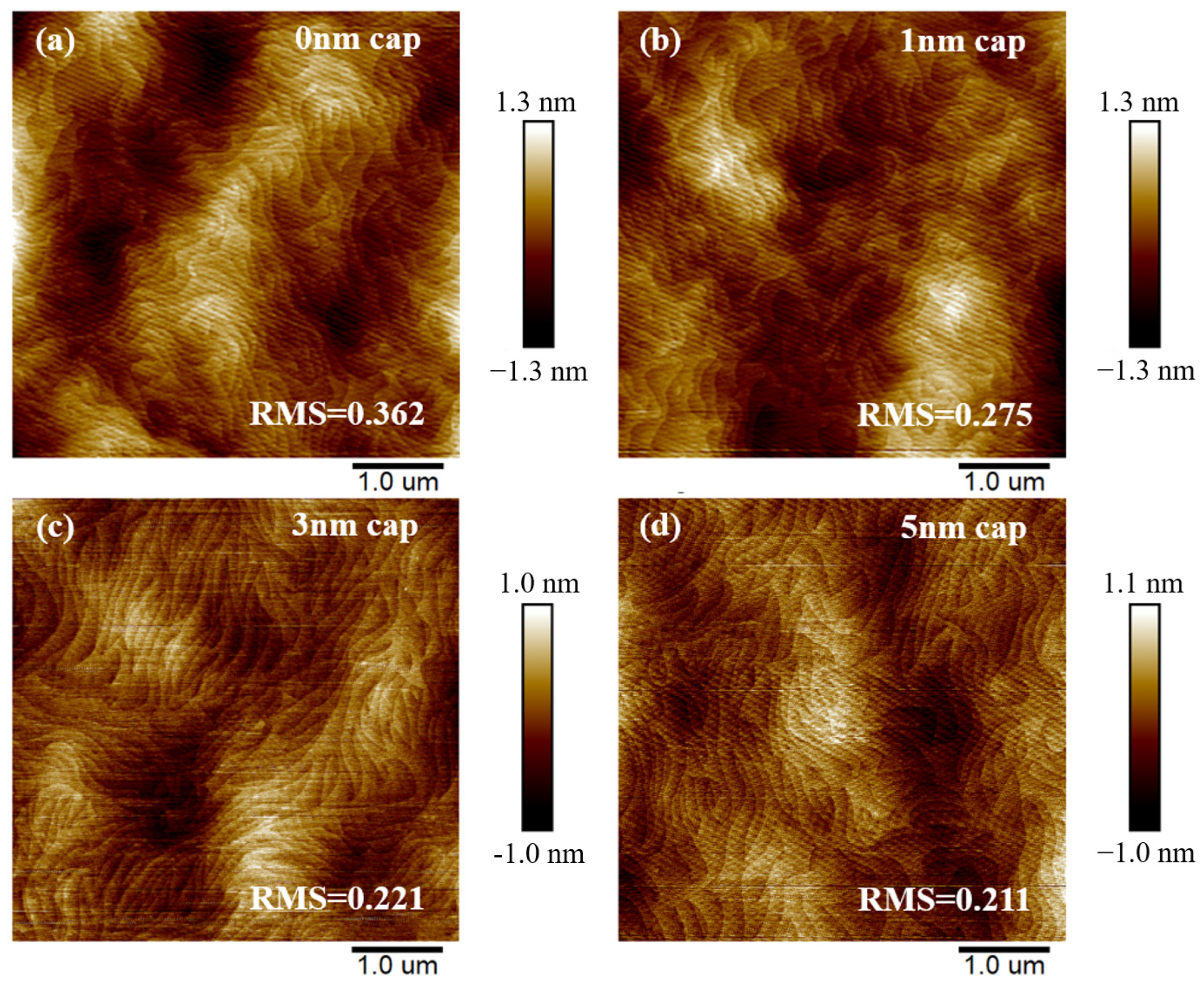
Figure 2a–d respectively show the AFM micrographs of samples with cap thickness of 0, 1, 3, and 5 nm. From Figure 2, the well-defined step flow morphology can be observed from the surfaces of these four samples. The obvious step flow morphology is the result of the high efficiency growth of the film. The root mean square (RMS) roughness of the sample surface was significantly reduced by the introduction of GaN. Similar observations have been documented in many studies [7]. A GaN cap layer can inhibit oxidation on the surface of the epitaxial layer, which may account for the reduced surface roughness. It was observed that as the cap thickness increased from 1 nm to 5 nm, the RMS of the wafer decreased from 0.275 nm to 0.211 nm, making the surface of the film even smoother. However, the surface roughness of a sample with a 5 nm cap is comparable to that of the sample with a 3 nm cap. We speculate that the protrusions on rough surfaces may hinder the lateral migration of Ga, leading to a tendency for GaN to form in the depressions, thus reducing the surface roughness of the film [15,16,17].
Figure 3 shows the values of 2DEG mobility (μH), 2DEG density (ns), and sheet resistance (Rs) of samples with cap thicknesses of 0, 1, 3, and 5 nm measured at 300 K. As the cap thickness increased from 0 nm to 5 nm, the ns decreased from 1.13 × 1013 cm−2 to 1.02 × 1013 cm−2. Due to the lattice mismatch between the GaN cap layer and the AlGaN barrier layer, the increase in cap thickness led to an enhanced piezoelectric polarization field above the barrier layer. This raised the conduction band and decreased the ns. As the cap thickness increased, the μH increased. The decrease in ns led to a reduction in the intensity of roughness scattering at the heterojunction interface [18,19]. In addition, as the cap thickness increased, the surface roughness of these samples decreased and the distance from the 2DEG to the surface of the epitaxial layer increased, which may lead to a decrease in remote scattering intensity from the surface charges [20,21]. In addition, the difference in μH between the sample with a 3 nm cap and the sample with a 5 nm cap was observed to be nonsignificant. We speculate that the lower ns led to a reduced effect of the ns change on the roughness scattering intensity of the heterogeneous interface. As the cap thickness increased, interface roughness scattering intensity and the remote scattering intensity from the surface charges decreased, which made the effect of both on the μH decrease. Therefore, the increase in mobility was no longer significant.
Figure 4 shows the output characteristic curves of these four samples. The IdSat of the devices with cap thickness of 0, 1, 3, and 5 nm are 358 mA/mm, 349 mA/mm, 343 mA/mm, and 319 mA/mm, respectively, at a gate-to-source voltage (VGS) of 2 V. As the cap thickness increased, the IdSat of the device decreased. However, as the cap thickness increased from 0 to 3 nm, the change in IdSat of the device was not significant. Although the 2DEG concentration decreased with the increase in cap thickness, a significant increase in carrier mobility was observed.
The transfer characteristics of these four samples are depicted in Figure 5. The Vth is defined as the drain voltage at which the drain current is 1 mA/mm. The Vth of samples with cap thickness of 0, 1, 3, and 5 nm are −2.92 V, −2.86 V, −2.8 V, and −2.8 V respectively. The Vth is the point at which a device transitions from an on-state to an off-state. Although the distance between the gate and the channel layer increased with increasing GaN cap thickness, making it more difficult to deplete the carrier in the channel, the reduced carrier density compensates for this effect and minimizes the variation in the Vth of all these samples. Therefore, the disparity in Vth among the samples is slight. The transconductance (Gm) of the devices with cap thicknesses of 0, 1, 3, and 5 nm are 96 mS/mm, 92 mS/mm, 86 mS/mm, and 77 mS/mm, respectively. The Gm is positively correlated with gate capacitance and carrier concentration. As the GaN cap thickness increased, the distance between the gate and the channel layer increased, resulting in a decrease in gate capacitance. Additionally, the decrease in ns further led to the decrease in Gm.
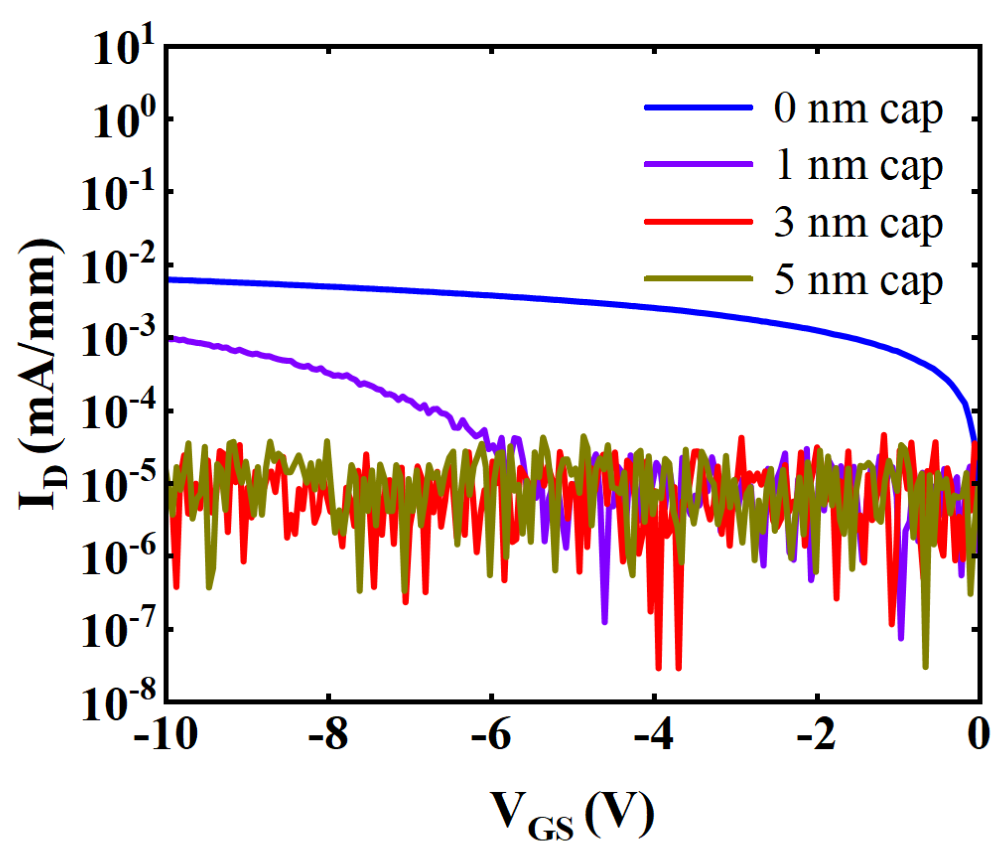
Figure 6 shows the drain current as a function of VGS expressed on a log scale. It was observed that the IdLeak of the device decreased as the cap thickness increased, and the IdLeak of the device decreased by about two orders of magnitude after the cap thickness increased from 0 to 3 nm. The drain current ON/OFF (Ion/Ioff) ratio of the devices with cap thickness of 3 nm and 5 nm were both higher than 107 due to the reduced IdLeak. Thus, the increased GaN cap thickness reduced the IdLeak and improved the Ion/Ioff ratio.
Figure 7 shows the gate leakage curves of samples with cap thickness of 0, 1, 3, and 5 nm. As the cap thickness increased, IgLeak decreased. To appreciate the effect of GaN cap thickness on the off-state characteristics of the device, simulation was performed using Silvaco TCAD 2014. Figure 8 shows the electric field distribution of the device under a biasing condition of VGS = −8 V, and VDS = 0 V. Figure 8a shows the electric field distribution of the device without GaN cap layer, where the electric field is concentrated at the gate edge due to the lateral electric field crowd. As shown in Figure 8b, the introduced GaN cap layer homogenized the electric field in the barrier layer, leading to a decrease in peak electric field [22]. The peak electric field decreased as the thickness of the GaN cap layer increased. We speculate that the negatively polarized electric field introduced by the GaN cap layer reduced the potential at the top of the barrier layer. It increased the vertical electric field in the GaN barrier layer, thus reducing the lateral electric field crowding [22,23,24,25]. As the thickness of the GaN cap increased, the potential at the top of the barrier layer further decreased and the electric field distribution further homogenized. Therefore, the increase in GaN cap thickness can effectively reduce the peak electric field near the gate. As the GaN cap thickness increased, the electric field peak in the barrier layer decreased and the barrier thickness increased, which effectively suppressed the vertical tunneling of electrons and thus reduced the IgLeak. The thick GaN cap layer also reduced the carrier density under the gate and improved the barrier thickness, which further inhibited the vertical tunneling of electrons. In addition, the GaN cap layer could also inhibit the natural oxidation of the epitaxial layer. The reduction of O impurities on the surface of the epitaxial layer could reduce the hopping probability of electrons through the defect state and further reduce the IgLeak [26,27,28].
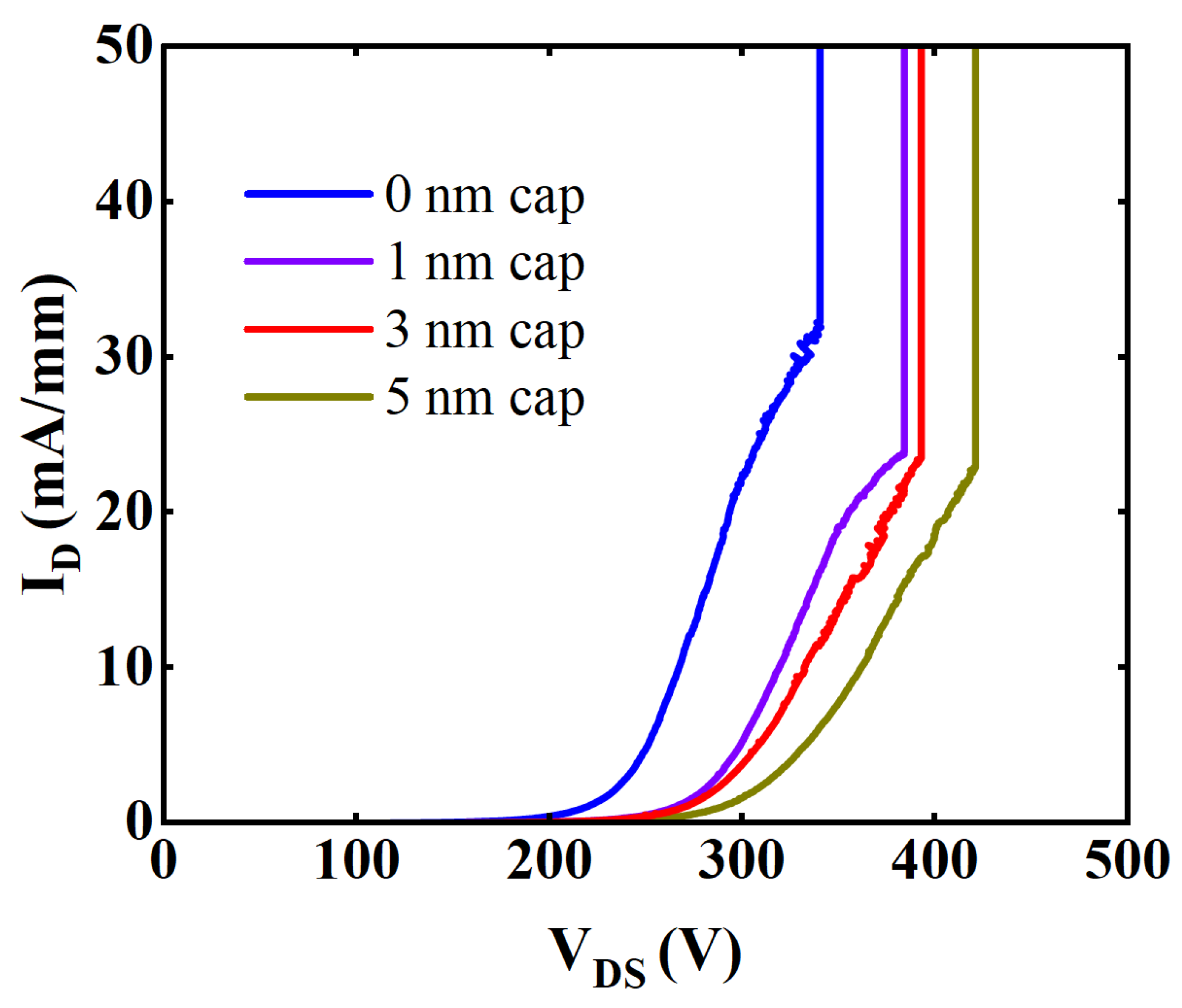
Figure 9 shows the breakdown characteristic curves of all these samples. It was observed that the BV of devices with cap thicknesses of 0, 1, 3, and 5 nm were 325 V, 383 V, 393 V, and 414 V respectively. As the cap thickness increased, the BV increased. As mentioned previously, the increase in GaN cap thickness inhibited the IgLeak and the IdLeak, resulting in an increase in BV.
4. Conclusions
We have investigated the material and electrical properties of AlGaN/GaN HEMTs with GaN cap thicknesses of 0, 1, 3, and 5 nm, respectively. Although the increased cap thickness causes a reduced carrier concentration, a too-thin GaN cap layer is not suitable as a cap for an HEMT. The too-thin GaN cap leads to an increase in the surface roughness of the epitaxial layer and a degradation in device off-state performance. A too-thick GaN cap layer significantly reduces the IdSat of the device. The optimized cap thickness was 3 nm. As the cap thickness increased from 0 to 3 nm, the surface roughness of the samples decreased from 0.362 nm to 0.221 nm. Meanwhile, IdSat decreased by less than 10%, while both IdLeak and IgLeak decreased by about 2 orders of magnitude, and BV increased by about 70 V. The results for the quantification and reproducibility of HEMT clearly indicate the role of GaN cap thickness.
Author Contributions
Conceptualization, Z.N.; methodology, Z.N. and K.W.; validation, Z.N.; formal analysis, Z.N. and X.L.; writing—original draft preparation, Z.N.; writing—review and editing, H.W.; supervision, H.W. All authors have read and agreed to the published version of the manuscript.
Funding
This work was supported by Science and Technology Plan Project of Guangdong Province (No.2020B010171001), and Guangzhou Municipal Science and Technology Plan Project (2021ZD001), and Science and Technology Development Special Fund Projects of Zhongshan City (Nos.2019AG014, 2019AG042, 2020AG023).
Data Availability Statement
The original contributions presented in the study are included in the article, further inquiries can be directed to the corresponding author.
Conflicts of Interest
The authors declare no conflicts of interest.
References
- Zhang, Y.; Zubair, A.; Liu, Z.; Xiao, M.; Perozek, J.; Ma, Y.; Palacios, T. GaN FinFETs and trigate devices for power and RF applications: Review and perspective. Semicond. Sci. Technol. 2021, 36, 054001. [Google Scholar] [CrossRef]
- Amano, H.; Baines, Y.; Beam, E.; Borga, M.; Bouchet, T.; Chalker, P.R.; Charles, M.; Chen, K.J.; Chowdhury, N.; Chu, R. The 2018 GaN power electronics roadmap. J. Phys. D Appl. Phys. 2018, 51, 163001. [Google Scholar] [CrossRef]
- Chen, K.J.; Häberlen, O.; Lidow, A.; lin Tsai, C.; Ueda, T.; Uemoto, Y.; Wu, Y. GaN-on-Si power technology: Devices and applications. IEEE Trans. Electron Devices 2017, 64, 779–795. [Google Scholar] [CrossRef]
- He, J.; Cheng, W.C.; Wang, Q.; Cheng, K.; Yu, H.; Chai, Y. Recent advances in GaN-based power HEMT devices. Adv. Electron. Mater. 2021, 7, 2001045. [Google Scholar] [CrossRef]
- Yu, E.; Dang, X.; Asbeck, P.; Lau, S.; Sullivan, G. Spontaneous and piezoelectric polarization effects in III–V nitride heterostructures. J. Vac. Sci. Technol. B 1999, 17, 1742–1749. [Google Scholar] [CrossRef]
- Jurkovic, M.; Gregusova, D.; Palankovski, V.; Hascik, Š.; Blaho, M.; Cico, K.; Frohlich, K.; Carlin, J.-F.; Grandjean, N.; Kuzmik, J. Schottky-barrier normally off GaN/InAlN/AlN/GaN HEMT with selectively etched access region. IEEE Electron Device Lett. 2013, 34, 432–434. [Google Scholar] [CrossRef]
- Arulkumaran, S.; Egawa, T.; Ishikawa, H. Studies on the influences of i-GaN, n-GaN, p-GaN and InGaN cap layers in AlGaN/GaN high-electron-mobility transistors. Jpn. J. Appl. Phys. 2005, 44, 2953. [Google Scholar] [CrossRef]
- Yoshida, S.; Sakaida, Y.; Asubar, J.; Tokuda, H.; Kuzuhara, M. Current collapse in AlGaN/GaN HEMTs with a GaN cap layer. In Proceedings of the 2015 IEEE International Meeting for Future of Electron Devices, Kansai (IMFEDK), Kyoto, Japan, 4–5 June 2015. [Google Scholar]
- Zhang, T.; Lv, Y.; Li, R.; Zhang, Y.; Zhang, Y.; Li, X.; Zhang, J.; Hao, Y. Current-collapse suppression of high-performance lateral AlGaN/GaN Schottky barrier diodes by a thick GaN cap layer. IEEE Electron Device Lett. 2021, 42, 477–480. [Google Scholar] [CrossRef]
- Hao, R.; Li, W.; Fu, K.; Yu, G.; Song, L.; Yuan, J.; Li, J.; Deng, X.; Zhang, X.; Zhou, Q. Breakdown enhancement and current collapse suppression by high-resistivity GaN cap layer in normally-off AlGaN/GaN HEMTs. IEEE Electron Device Lett. 2017, 38, 1567–1570. [Google Scholar] [CrossRef]
- Nishiguchi, K.; Nakata, K.; Nishiguchi, N.; Hashizume, T. Effects of a GaN cap layer on admittance characteristics of AlGaN/GaN MIS structures. J. Appl. Phys. 2023, 134, 055702. [Google Scholar] [CrossRef]
- Kikkawa, T.; Nagahara, M.; Okamoto, N.; Tateno, Y.; Yamaguchi, Y.; Hara, N.; Joshin, K.; Asbeck, P. Surface-charge controlled AlGaN/GaN-power HFET without current collapse and gm dispersion. In Proceedings of the International Electron Devices Meeting. Technical Digest (Cat. No. 01CH37224), Washington, DC, USA, 2–5 December 2001. [Google Scholar]
- Sfuncia, G.; Nicotra, G.; Giannazzo, F.; Pécz, B.; Gueorguiev, G.K.; Kakanakova-Georgieva, A. 2D graphitic-like gallium nitride and other structural selectivity in confinement at the graphene/SiC interface. CrystEngComm. 2023, 25, 5810–5817. [Google Scholar] [CrossRef]
- Li, Y.; Wu, Y.; Ding, S. First principle studies of oxygen absorption on GaN (0001) surface with steps. Phys. Rev. B Condens. Matter 2022, 627, 413528. [Google Scholar] [CrossRef]
- Narang, K.; Bag, R.K.; Singh, V.K.; Pandey, A.; Saini, S.K.; Khan, R.; Arora, A.; Padmavati, M.; Tyagi, R.; Singh, R. Improvement in surface morphology and 2DEG properties of AlGaN/GaN HEMT. J. Alloys Compd. 2020, 815, 152283. [Google Scholar] [CrossRef]
- Valipa, M.S.; Sriraman, S.; Aydil, E.S.; Maroudas, D. Atomic-scale analysis of fundamental mechanisms of surface valley filling during plasma deposition of amorphous silicon thin films. Surf. Sci. 2005, 574, 123–143. [Google Scholar] [CrossRef]
- Sharma, N.; Thomas, P.; Tricker, D.; Humphreys, C. Chemical mapping and formation of V-defects in InGaN multiple quantum wells. Appl. Phys. Lett. 2000, 77, 1274–1276. [Google Scholar] [CrossRef]
- Katz, O.; Horn, A.; Bahir, G.; Salzman, J. Electron mobility in an AlGaN/GaN two-dimensional electron gas. I. Carrier concentration dependent mobility. IEEE Trans. Electron Devices 2003, 50, 2002–2008. [Google Scholar] [CrossRef]
- Lee, G.Y.; Tu, P.T.; Chyi, J.I. Improving the off-state characteristics and dynamic on-resistance of AlInN/AlN/GaN HEMTs with a GaN cap layer. Appl. Phys. Express 2015, 8, 064102. [Google Scholar] [CrossRef]
- Yaita, J.; Yamada, A.; Nakamura, N.; Kotani, J. Probing the effects of surface roughness and barrier layer thickness in InAlGaN/GaN HEMTs to improve carrier mobility. Appl. Phys. Express 2021, 14, 031005. [Google Scholar] [CrossRef]
- Zhao, J.-T.; Lin, Z.-J.; Luan, C.-B.; Lü, Y.-J.; Feng, Z.-H.; Yang, M. Effects of GaN cap layer thickness on an AlN/GaN heterostructure. Chin. Phys. B 2014, 23, 127104. [Google Scholar] [CrossRef]
- Sarkar, S.; Khade, R.P.; DasGupta, A.; DasGupta, N. Effect of GaN cap layer on the performance of AlInN/GaN-based HEMTs. Microelectron. Eng. 2022, 258, 111756. [Google Scholar] [CrossRef]
- Wuerfl, J.; Bahat-Treidel, E.; Brunner, F.; Cho, E.; Hilt, O.; Ivo, P.; Knauer, A.; Kurpas, P.; Lossy, R.; Schulz, M. Reliability issues of GaN based high voltage power devices. Microelectron. Reliab. 2011, 51, 1710–1716. [Google Scholar] [CrossRef]
- Duan, B.; Yang, L.; Wang, Y.; Yang, Y. Experimental results for AlGaN/GaN HEMTs improving breakdown voltage and output current by electric field modulation. IEEE Trans. Electron Devices 2021, 68, 2240–2245. [Google Scholar] [CrossRef]
- Yang, L.; Duan, B.; Dong, Z.; Wang, Y.; Yang, Y. The analysis model of AlGaN/GaN HEMTs with electric field modulation effect. IETE Tech. Rev. 2020, 37, 553–564. [Google Scholar] [CrossRef]
- Goyal, A.; Yadav, B.S.; Raman, R.; Kumar, A.; Dalal, S.; Tyagi, R.; Kumar, V.; Kapoor, A.K. Non Destructive Evaluation of AlGaN/GaN HEMT structure by cathodoluminescence spectroscopy. J. Lumin. 2021, 232, 117834. [Google Scholar] [CrossRef]
- Wu, N.; Luo, L.; Xing, Z.; Li, S.; Zeng, F.; Cao, B.; Wu, C.; Li, G. Enhanced Performance of Low-Leakage-Current Normally off p-GaN Gate HEMTs Using NH3 Plasma Pretreatment. IEEE Trans. Electron Devices 2023, 68, 2240–2245. [Google Scholar] [CrossRef]
- Tajima, M.; Kotani, J.; Hashizume, T. Effects of surface oxidation of AlGaN on DC characteristics of AlGaN/GaN high-electron-mobility transistors. Jpn. J. Appl. Phys. 2009, 48, 020203. [Google Scholar] [CrossRef]
Figure 1.
Schematic cross-section of HEMTs.

Figure 2.
AFM image (scan area = 5 μm × 5 μm) of samples with cap thickness of (a) 0 nm, (b) 1 nm, (c) 3 nm, (d) 5 nm.
Figure 2.
AFM image (scan area = 5 μm × 5 μm) of samples with cap thickness of (a) 0 nm, (b) 1 nm, (c) 3 nm, (d) 5 nm.

Figure 3.
The room temperature Hall test results for samples with cap thickness of 0, 1, 3, and 5 nm.
Figure 3.
The room temperature Hall test results for samples with cap thickness of 0, 1, 3, and 5 nm.

Figure 4.
Output characteristics of samples with cap thickness of (a) 0 nm, (b) 1 nm, (c) 3 nm, and (d) 5 nm.
Figure 4.
Output characteristics of samples with cap thickness of (a) 0 nm, (b) 1 nm, (c) 3 nm, and (d) 5 nm.

Figure 5.
Transfer characteristics of samples with cap thickness of 0, 1, 3, and 5 nm.

Figure 6.
Transfer characteristics of samples with cap thicknesses of 0, 1, 3, and 5 nm with drain current on a log scale.
Figure 6.
Transfer characteristics of samples with cap thicknesses of 0, 1, 3, and 5 nm with drain current on a log scale.

Figure 7.
Off-state gate leakage characteristics of samples with cap thickness of 0 nm, 1 nm, 3 nm, and 5 nm.
Figure 7.
Off-state gate leakage characteristics of samples with cap thickness of 0 nm, 1 nm, 3 nm, and 5 nm.

Figure 8.
Simulated electric field profile under the gate at a biasing condition of VGS = −8 V, and VDS = 0 V, with embedded figure of peak electric field against cap thickness.
Figure 8.
Simulated electric field profile under the gate at a biasing condition of VGS = −8 V, and VDS = 0 V, with embedded figure of peak electric field against cap thickness.

Figure 9.
Breakdown characteristics of samples with cap thickness of 0, 1, 3, and 5 nm.

Disclaimer/Publisher’s Note: The statements, opinions and data contained in all publications are solely those of the individual author(s) and contributor(s) and not of MDPI and/or the editor(s). MDPI and/or the editor(s) disclaim responsibility for any injury to people or property resulting from any ideas, methods, instructions or products referred to in the content. |
© 2024 by the authors. Licensee MDPI, Basel, Switzerland. This article is an open access article distributed under the terms and conditions of the Creative Commons Attribution (CC BY) license (https://creativecommons.org/licenses/by/4.0/).
Share and Cite
MDPI and ACS Style
Nie, Z.; Wang, K.; Liu, X.; Wang, H. Effect of GaN Cap Thickness on the DC Performance of AlGaN/GaN HEMTs. Micromachines 2024, 15, 571. https://0-doi-org.brum.beds.ac.uk/10.3390/mi15050571
AMA Style
Nie Z, Wang K, Liu X, Wang H. Effect of GaN Cap Thickness on the DC Performance of AlGaN/GaN HEMTs. Micromachines. 2024; 15(5):571. https://0-doi-org.brum.beds.ac.uk/10.3390/mi15050571
Chicago/Turabian StyleNie, Zuorong, Kai Wang, Xiaoyi Liu, and Hong Wang. 2024. "Effect of GaN Cap Thickness on the DC Performance of AlGaN/GaN HEMTs" Micromachines 15, no. 5: 571. https://0-doi-org.brum.beds.ac.uk/10.3390/mi15050571
Note that from the first issue of 2016, this journal uses article numbers instead of page numbers. See further details here.