
Wideband Millimeter-Wave Perforated Hemispherical Dielectric Resonator Antenna

1
Communications Research Group, Department of Electronic and Electrical Engineering, University of Sheffield, Sheffield S1 3JD, UK
2
Department of Mechanical Engineering, University of Sheffield, Sheffield S1 3JD, UK
*
Author to whom correspondence should be addressed.
Electronics 2024, 13(9), 1694; https://0-doi-org.brum.beds.ac.uk/10.3390/electronics13091694
Submission received: 22 March 2024
/
Revised: 23 April 2024
/
Accepted: 26 April 2024
/
Published: 27 April 2024
(This article belongs to the Special Issue Smart Communication and Networking in the 6G Era)
Abstract
:This paper presents a novel wideband circularly polarized millimeter-wave (mmWave) hemispherical dielectric resonator antenna (HDRA). Two distinct configurations of alumina dielectric resonator antennas (DRAs) are investigated, each featuring a different coating: the first configuration incorporates a polyimide layer, while the second involves a perforated alumina. Both configurations demonstrate promising characteristics, including impedance and axial ratio (AR) bandwidths of 58% and 17.7%, respectively, alongside a maximum gain of 10 dBic at 28 GHz. Leveraging additive manufacturing technology, the HDRA with the perforated coating layer is fabricated, simplifying assembly and eliminating potential air gaps between layers, thereby enhancing the overall performance. This innovative approach yields a circularly polarized (CP) HDRA suitable for Beyond 5G (B5G) communication systems. Agreement between measurements and simulations validates the efficacy of the proposed design, affirming its potential in practical applications.
1. Introduction
Due to the promising applications in 5G and beyond communication systems, there has been a notable surge in research interest in millimeter-wave frequencies, particularly in developing wideband efficient antennas. However, challenges persist in the design of mmWave antennas, primarily stemming from significant signal attenuation, necessitating the utilization of high-gain antennas. Additionally, the potential escalation of ohmic losses in metal antennas and array feed networks poses concerns, leading to compromised radiation efficiency and gain [1]. Furthermore, microstrip antennas suffer from narrow impedance bandwidths typically ranging from 2% to 5% [2]. To address these limitations, DRAs have emerged as a viable solution, offering enhanced gain and expanded bandwidth. DRAs possess several advantageous characteristics, including compact size, versatility in shapes, flexible excitation mechanisms, low profile, and lightweight nature [3,4].
While single-layer hemispherical DRAs have been extensively studied across various frequency bands, employing techniques such as a probe or conformal strip feeding, challenges arise when operating at mmWave frequencies. Probe feeding, for instance, becomes impractical due to the necessity of drilling holes in physically small ceramic structures, risking damage to the antenna or significant air-gap sizes relative to the shorter wavelengths [5]. Conversely, slot feeding emerges as a more favorable option at higher frequencies, given its ease of fabrication and the ability to isolate the antenna from the feed network, thereby minimizing spurious radiation. Furthermore, the resonance modes of isolated hemispherical DRAs can be numerically determined by solving the characteristic mode equation, assuming placement on an infinite perfectly conducting ground plane. These resonance modes can be categorized into two primary groups: Transverse Electric (TEₘₙₛ) and Transverse Magnetic (TMₘₙₛ) modes, with TE111 and TM101 representing the fundamental modes. The radiation pattern of the TE111 mode resembles that of a short horizontal magnetic dipole, while the TM101 mode exhibits characteristics akin to a short electric monopole. Consequently, the diverse array of modes renders the hemispherical DRA (HDRA) appealing for various applications. The subscripts n, m, and s denote variations in fields along the elevation (θ), azimuth (ϕ), and radial (r) axes of the spherical coordinate system.
It is well known that a substantial increase in the impedance bandwidth can be achieved by appending a dielectric coat to the DRA [6] since it acts as a transition zone between the antenna and the free space. Recent reports indicate that the DRA coating can increase gain, circular polarization, and impedance bandwidths [7,8]. As an example, a wideband slot-fed multi-layer hemispherical DRA has been reported with an impedance bandwidth of 55% by exciting the TE111 and TE221 resonance modes in combination with the slot’s resonance mode [9]. There have also been suggestions that a coaxial probe fed three-layer hemispherical DRA can be adopted in conjunction with materials that have relative permittivities of 9, 4 and 3 for the inner, middle, and outer layers, respectively, wherein a bandwidth of 65.6% has been realized with a lower gain of 3.2 dBi when lower-order modes of TM101 and TM102 are excited [10]. However, as mentioned earlier, probe feeding is impractical at mmWave frequencies. An alternative design of a three-layer hemispherical DRA has been reported using a rectangular waveguide feed whereby the optimization of the outer layer’s permittivity renders the possibility of a broadband coupling to deliver impedance bandwidth and gain of 9.6% and 6.4 dBi, respectively, through the excitation of the TE113 mode [11]. Another research study reported a wide impedance bandwidth of ~25% in cases where a conformal strip is employed to excite a three-layer hemispherical DRA operating in the TE111 fundamental mode [12]. A hemispherical DRA on a ground plane, fabricated using 3D printing technology with a conductive material, is presented in [13]. The antenna is optimized for operation in the C-band. Performance analysis reveals a bandwidth of return losses reaching 12.2%, along with an average and peak gain of 4.69 dBi. However, it is noted that utilizing probe feeding may significantly impact the antenna’s bandwidth and efficiency, particularly in mmWave design scenarios. In [14], another design employing probe feeding is introduced. It explores a multi-layered cylindrical dielectric resonator antenna crafted with 3D-printing technology and tested at X-band frequencies. This design offers an impedance bandwidth of 65.7% (3.56–7.04 GHz) with a gain of 2.3 dB. However, it is difficult to precisely fix a conformal strip on the DRA surface at mmWave frequencies due to the smaller dimensions and potential air gaps between the strip and DRA. Another slot-coupled three-layer hemispherical DRA design offers a broad impedance bandwidth in the region of 29% with a gain of 4.4 dBi proposed by exciting the fundamental TE111 resonance mode [15]. When the performance of a two-layer hemispherical DRA is compared to that of a single-layer counterpart, it becomes evident that there is a broader bandwidth of 31.9% and a gain of 2.5 dBi for the layered DRA compared to 14% for the single-layer DRA that operates at the TM101 lower order mode [16]. On the other hand, multi-layer DRA configurations are associated with known limitations, such as the increased physical size and the complex assembly procedure with respect to bonding the different dielectric layers together with no potential air gaps in between. This study addresses the above issue by utilizing 3D printing technology to fabricate a DRA and perforated coat configuration using alumina. It should be noted that innovative 3D printing technology is simple, cost-effective, and has a short fabrication cycle. Hence, it has recently been considered in the context of DRA fabrications as it eliminates the potential air gaps more effectively than other fabrication techniques [17,18].
In this paper, we introduce a novel approach wherein the traditional layered hemispherical dielectric resonator antenna (DRA) geometry is replaced with an alumina structure comprising two distinct sections: an inner solid DRA and an outer perforated coat featuring a considerably lower effective dielectric constant. This structural modification enables an automated 3D printing process, obviating the requirement for labor-intensive assembly and bonding of numerous solid dielectric layers. Moreover, utilizing the same material for both the DRA and the coat optimizes the 3D printing procedure, thereby enhancing overall efficiency.
It is noteworthy that prior research, as documented in [19], has introduced a 3D-printed cylindrical DRA with a perforated coat, achieving optimal performance through the utilization of a cross-slot topped by a thin alumina layer to enhance coupling. Conversely, in our proposed hemispherical DRA (HDRA), optimal performance is attained through the implementation of a spiral slot. This discrepancy in performance stems from variations in the electromagnetic field distribution within the two DRAs. Additionally, the perforated coat layers exhibit differing numbers and sizes of air gaps in the respective DRAs. Consequently, maximum coupling to the HDRA is achieved without necessitating the addition of a thin alumina layer between the HDRA and the spiral slot.
Previous research on multi-layer hemispherical DRAs has primarily focused on enhancing impedance bandwidth, overlooking opportunities to widen the CP bandwidth, despite the potential afforded by the outer section to introduce an additional degree of freedom. Another contributing factor to the expanded CP bandwidth is the incorporation of an Archimedean spiral slot to feed the antenna, which excites multiple higher-order modes. Operating within the 18.4–33.4 GHz mmWave frequency band, the antenna demonstrates impressive impedance and axial ratio bandwidths of approximately 58% and 17%, respectively, surpassing those reported in earlier studies for circularly polarized hemispherical DRAs.
The paper is organized as follows: Section 2 introduces the proposed two configurations of the HDRA; Section 3 presents the measured results obtained from prototypes of the two HDRA configurations; and Section 4 offers concluding remarks and summaries. Simulations were conducted using CST Microwave Studio version 2020, and the results closely aligned with experimental measurements.
2. Antenna Configuration
Figure 1 illustrates the two-layer hemispherical DRA and feed network configurations proposed in this study, where the inner and outer layers have respective dielectric constants and radii of , a1 and , a2. For a single-layer HDRA, i.e., = 1, the resonant frequency of the fundamental mode TE111 can be determined by solving the mode characteristics equation [20,21].
in which , , , where and represent the spherical Bessel and Hankel functions of the 1st kind and the 2nd kind, respectively. To find the resonant frequency, Equation (1) is solved for a given a, from which k0 can be determined. Finally, the resonant frequency can be calculated as [22]
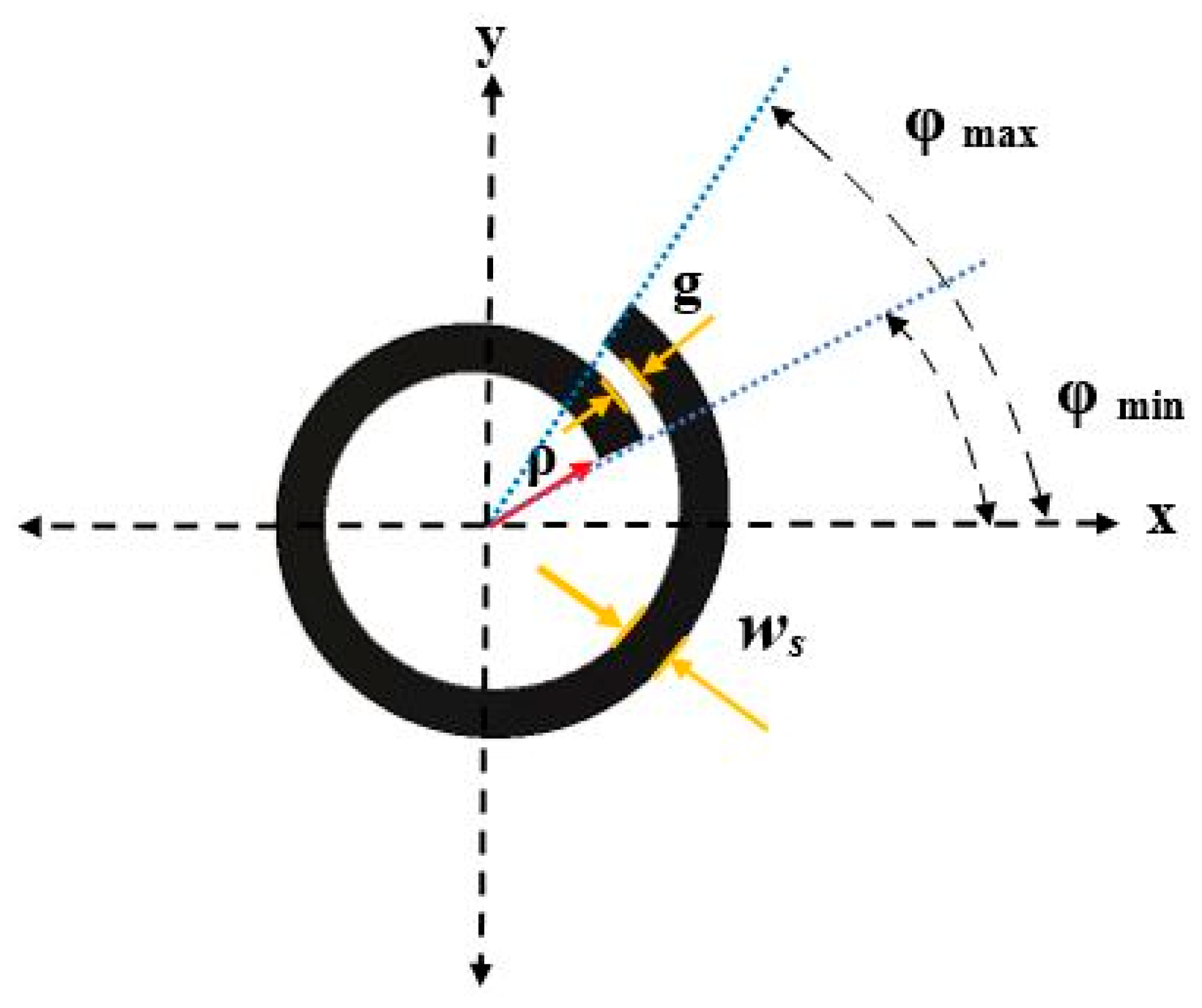
The feeding spiral is illustrated in Figure 2 with dimensions defined by the well-known Archimedean spiral function of [23]
where р ρ represents the radius of the spiral-slot arm, α is the spiral constant, and φ is the winding angle. The chosen parameters are α = 0.08 mm/rad, 0.138π ≤ φ ≤ 2.16π and the width of the spiral-slot arm is ws = 0.38 mm, which results in a spiral-slot arm length of 3.9 mm that is approximately 0.7λeff at an operating frequency of 29 GHz. The variations of the above spiral’s parameters and the separation between the spiral slot arm tuns (g) can change the spiral’s arm length and provide optimum impedance matching.
р = α φ
2.1. A Single-Layer HDRA
As a reference, a single-layer hemispherical DRA was initially examined, employing dielectric constants of and , with a radius of =3.8 mm.
The proposed antenna was placed on a 45 × 45 mm2 ground plane printed on a thin Rogers RO4350 dielectric substrate, featuring a thickness and dielectric constant of 0.42 mm and 3.48, respectively.
A feeding microstrip line was positioned on the lower side of the dielectric substrate, measuring 22.5 mm in length and 0.88 mm in width, tailored for optimal impedance matching.
Resonance modes of the single-layer DRA were determined by solving Equations (1) and (2) utilizing MATLAB (2021) code. For the specified dielectric constants, radius, feeding slot, and frequency range, the single-layer HDRA supported dual resonance modes, namely TE112 and TE511, at 25 GHz and 30.8 GHz, respectively. Figure 3 illustrates the performance, showcasing the achievement of a dual-band with impedance bandwidths of 19.29% and 9.37%, spanning frequencies from 24.3 to 29.6 GHz and 30.5 to 33.5 GHz, respectively. The simulated axial ratio bandwidth was obtained over a frequency range of 28.3–29.5 GHz, corresponding to 4.2%. These bandwidths were attained with a broadside gain of 5.7 dBic.
2.2. HDRA of Two Solid Dielectric Layers
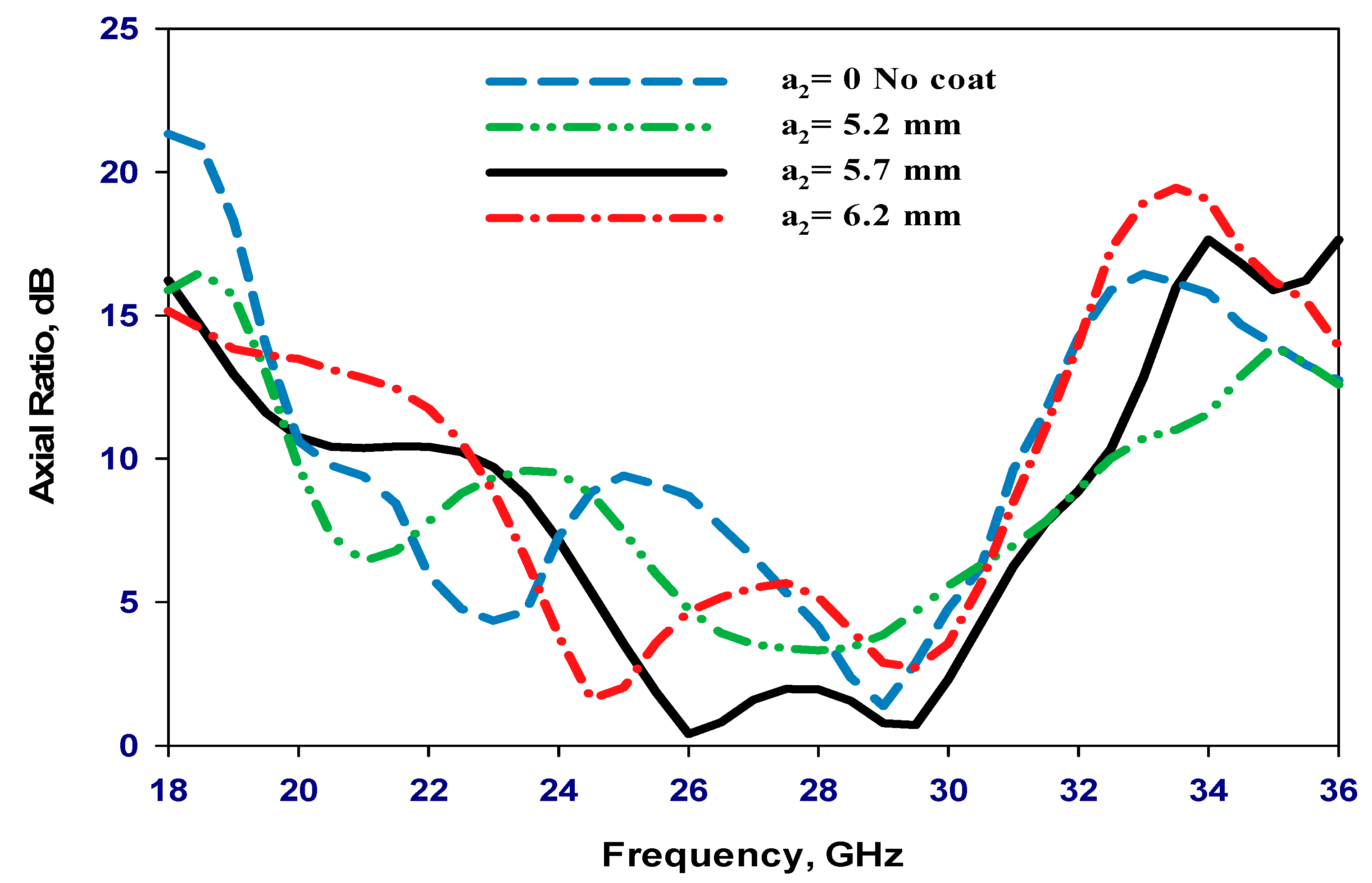
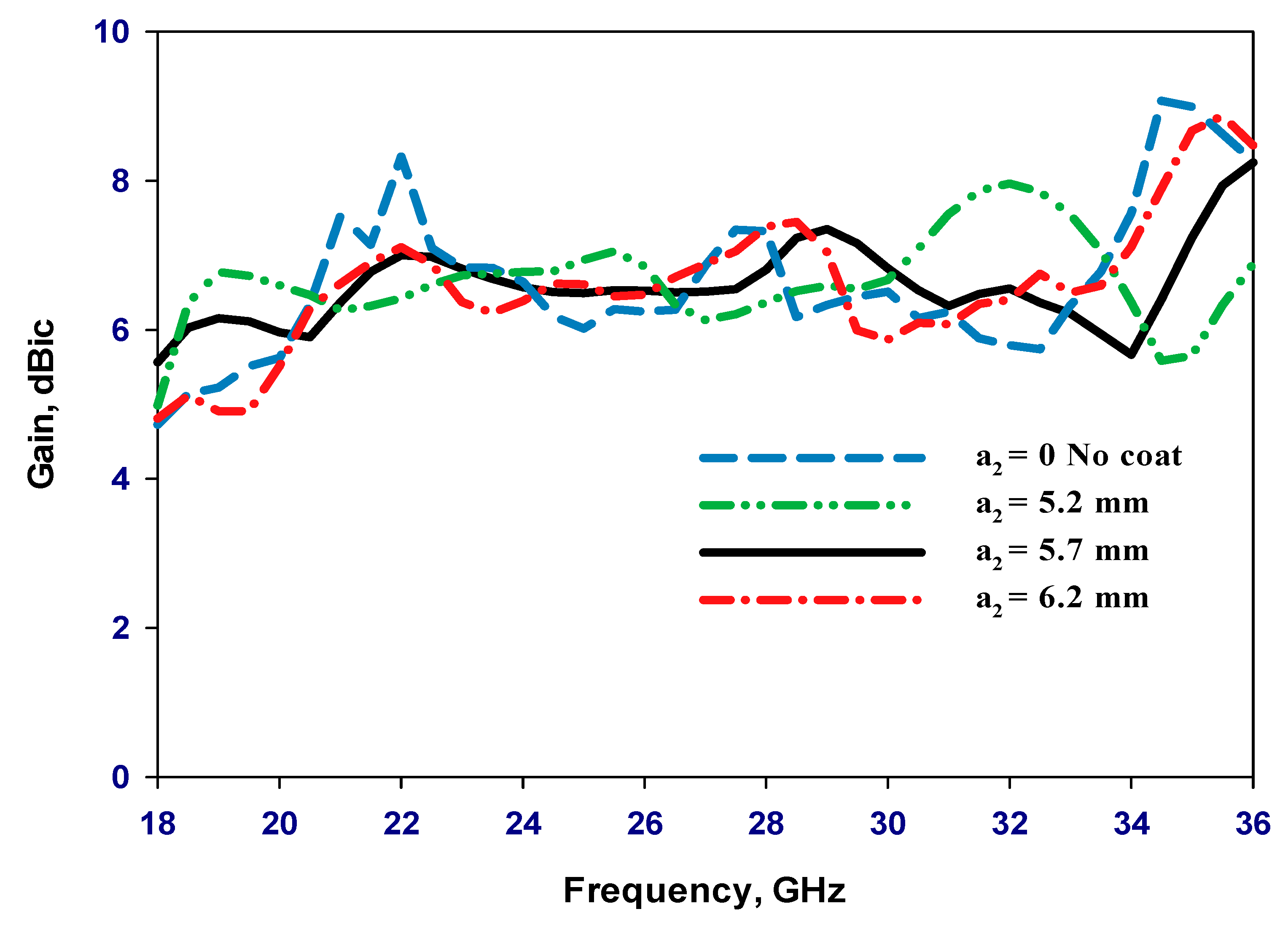
To enhance the impedance and AR bandwidths, the single-layer hemispherical DRA has been coated by a lower permittivity dielectric layer as illustrated in Figure 1. The coating layer’s dielectric constant needs to be less than that of the DRA so that the coat acts as a transition layer between the DRA and free space. With optimized coat thickness, the wave reflections at the DRA surface can be minimized, which results in an enhanced bandwidth. However, the choice of the outer layer’s dielectric constant is limited by the availability of commercial materials. Therefore, a polyimide layer has been utilized with a dielectric constant of = 3.5. On the other hand, the outer layer thickness of δa = a2 − a1 was increased from 0.9 to 2.4 mm. A comparison of the effects of different outer layer thicknesses on the reflection coefficient is presented in Figure 4. From these results, it can be noted that the widest impedance bandwidth was observed when the outer layer thickness is 1.9 mm and the narrowest bandwidth appeared when it was 1.4 mm. Figure 5 illustrates that the widest AR bandwidth is also achieved when an outer layer thickness is 1.9 mm. On the other hand, an outer layer thickness of 1.4 mm yielded the narrowest AR bandwidth. Based on Figure 4, Figure 5 and Figure 6, it was found that using a dielectric coat thickness of 1.9 mm results in significant improvements in impedance and axial ratio bandwidths. This is because with such a coat, the DRA excites the following resonance modes: TE311, TE112, TE511, and TE312 at 19 GHz, 24.6 GHz, 28.6 GHz, and 33.4 GHz, respectively, with an overall bandwidth of 57% spanning from 18.6 to 33.5 GHz. Therefore, a thickness of 1.9 mm, which corresponds to a2 = 5.7 mm, has been used for the outer layer. Furthermore, Figure 7 illustrates the variation in S11 bandwidth as a function of the coating thickness with the maximum bandwidth achieved using the same outer layer thickness of 1.9 mm.
2.3. Layered HDRA Using Alumina with a Perforated Coat
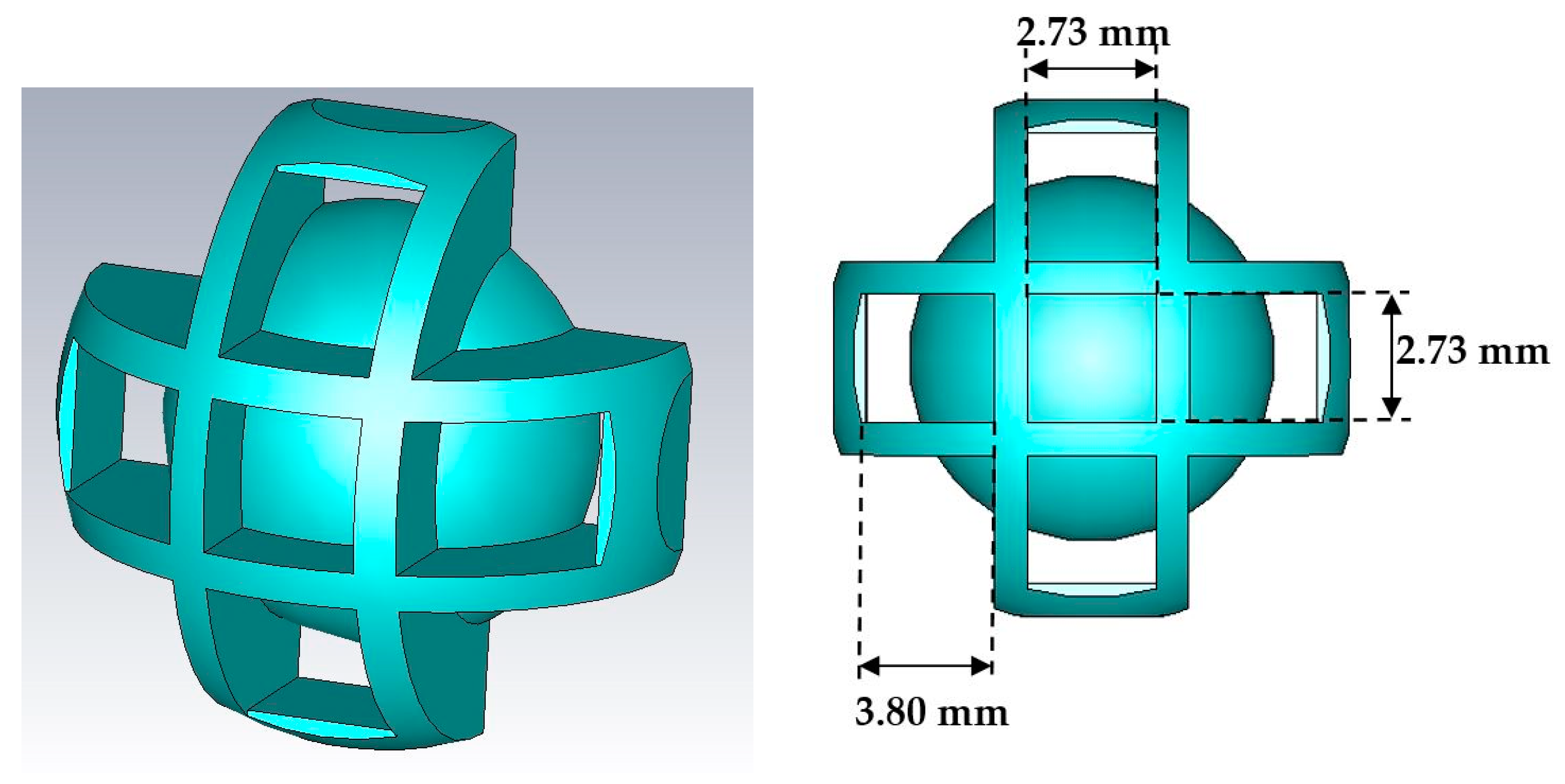
An equivalent configuration to the presented layered HDRA has been created, which consists of a physically single alumina layer with a top perforated section extending to a depth equal to the thickness of the polyimide coat presented in the previous section. This approach makes it easier to fabricate the proposed mmWave hemispherical DRA in accordance with the FDM 3D-printing technology. Therefore, no physical assembly of the two layers is needed, and there are no potential air gaps since alumina was used for the DRA and coat. Moreover, it is possible to realize the different dielectric constants of the dielectric coat by using different hole sizes, as per the filling-ratio theory [24]. The proposed 3D-printable HDRA is illustrated in Figure 8, which reveals that the DRA comprises two concentric alumina sections. Specifically, the outer section is characterized by different air-filling ratios designed to deliver diverse effective dielectric constants of the coating layer [25]. It should be noted that the DRA and coat dimensions, as well as the feed network of the previous section, have been utilized in the proposed configuration. Figure 9 demonstrates the overall 3D-printing compatible antenna.
A cubic unit cell with a dielectric constant of εr1, i.e., the same as that of the DRA, was introduced to create the perforated coat. The unit cell is intended to secure an effective dielectric constant of εr2eff for the perforated coat that can be calculated using [17].
εr2eff = 0.55tcεr1 − 0.04εr1 + 1.3
The unit cell has a side length of 2.73 mm, or 0.254λ0, where λ0 denotes the free space wavelength at 28 GHz and a wall thickness of tc. The unit cells possess the intrinsic capacity to provide mutual structural support, eliminating the necessity for supplementary support materials during the 3D printing process. As a direct outcome, there is a substantial diminution in both printing duration and material expenditure. The control over the effective permittivity of a perforated dielectric coat can be exercised by modulating the wall thickness as stipulated in Equation (4). The influence of the unit cells’ thickness was explored over a tc range of 0.59 to 0.79 mm, progressing in increments of 0.1 mm, in a hemispherical DRA design adorned with a perforated dielectric coat.
As illustrated in Figure 10, approximately the same S11 bandwidths were achieved using wall thicknesses of 0.59 and 0.69 mm, which are wider than that achieved using a thickness of 0.79 mm. Figure 11 corroborates these findings in the context of AR bandwidth (AR BW), revealing the maximum AR BW is achieved using a tc = 0.69 mm, whilst the most restricted AR BW was associated with tc = 0.59 mm. The impact of the wall thickness on the gain is distinctly depicted in Figure 12 with the highest gain achieved using tc = 0.69 mm. According to Equation (4), this is expected since a wall thickness of 0.69 mm provides the required effective permittivity of 3.5 for the perforated coat. It should be noted that the 3D printable antenna offers a maximum broadside gain of 9.5 dBic compared to 8.5 dBic achieved with an equivalent HDRA configuration of physically two dielectric layers. This demonstrates that the perforated coat has helped focus the main beam. Figure 13 compares the return losses of the original structure of two solid layers and that of the 3D-printed HDRA version, underlining the close congruity between the two configurations. For example, the configuration with a perforated coat has achieved an impedance bandwidth of ~58% compared to 57% for the two-layer structure.
3. Measurements and Discussions
To validate the simulation results, two prototypes of the HDRA with solid and perforated coatings were fabricated and measured. Each prototype was mounted on a Ro4350B dielectric substrate, which had a thickness of 0.42 mm, a permittivity of 3.48, and a loss tangent of 0.0037, provided by Wrekin Circuits. The antenna was fed using a microstrip line positioned beneath the Rogers substrate. A 2.4 mm SMA connector was employed to connect the feeding microstrip line to the Agilent Technologies E5071C mm-wave vector network analyzer via a 50 ohm coaxial cable. Radiation pattern measurements were conducted using an SNF-FIX-1.0 near-field system [26].
3.1. An HDRA Prototype with a Polyimide Coating
The hemispherical DRA element has been manufactured by the T-CERAM company (Hradec Králové, Czech Republic) using alumina with a fabrication tolerance of 0.06 mm as well as a dielectric constant of = 10 and loss tangent of tan δ < 0.002. The antenna’s coat layer has been fabricated with the aid of 3D-printing technology at the Protolabs Company (Maple Plain, MN, USA) using polyimide material with a dialectic constant of 3.5 and a loss tangent of 0.0027. The antenna and its feed network are illustrated in Figure 14. The simulated and measured reflection coefficients are depicted in Figure 15 with close agreement between simulated and measured impedance bandwidths of 57% and 51%, respectively, with a marginal discrepancy that can be attributed to the measurements and fabrication error. These results demonstrate that a layered DRA supports a multimode operation, where the resonance modes of TE311, TE112, TE511, and TE312 have been excited at 19 GHz, 24.6 GHz, 28.6 GHz, and 33.4 GHz, respectively. In addition, Figure 16 demonstrates that adding the outer dielectric layer enhances the AR bandwidth to ~18.2% over simulated and measured frequency ranges of 25.16 to 30.17 GHz and 25 to 30.6 GHz, respectively. Furthermore, the bandwidth improvement in the presence of the dielectric coat layer can be attributed to minimizing wave reflections at the coat–air interface, which lowers the quality factor of the antenna.
Figure 17 presents the layered DRA’s gain as a function of frequency, from which it can be noted that the maximum gain has been achieved at 29 GHz with simulated and measured peaks of 7.57 dBic and 6.9 dBic, respectively. It should be noted that the maximum gain has been achieved when the higher-order resonance mode, TE511, is excited. It is worth pointing out that the drop in the measured gain could be attributed to experimental errors such as losses in the cables, SMA soldering as well as the alignment in the anechoic chambers. Figure 18 illustrates good agreement between the simulated and measured H-plane and E-plane radiation patterns at 22 GHz and 29 GHz, respectively.
3.2. An HDRA Prototype with a Perforated Coat Layer
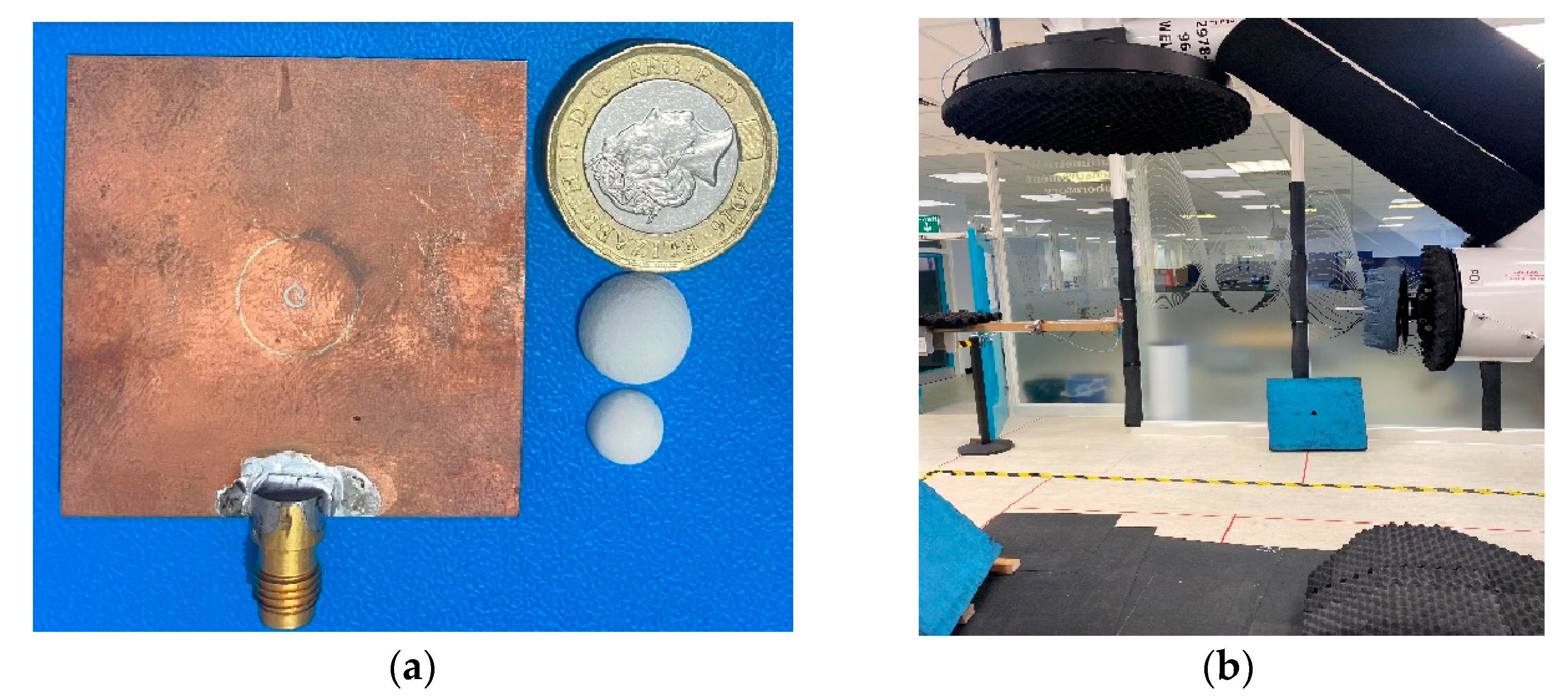
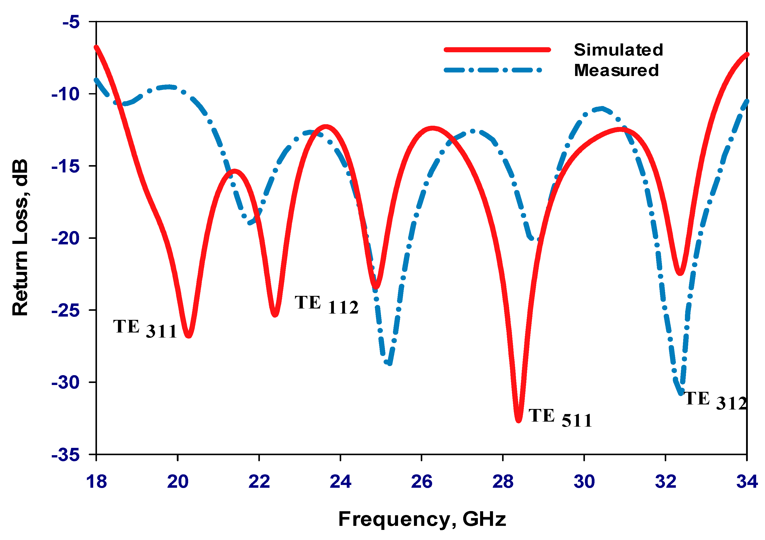
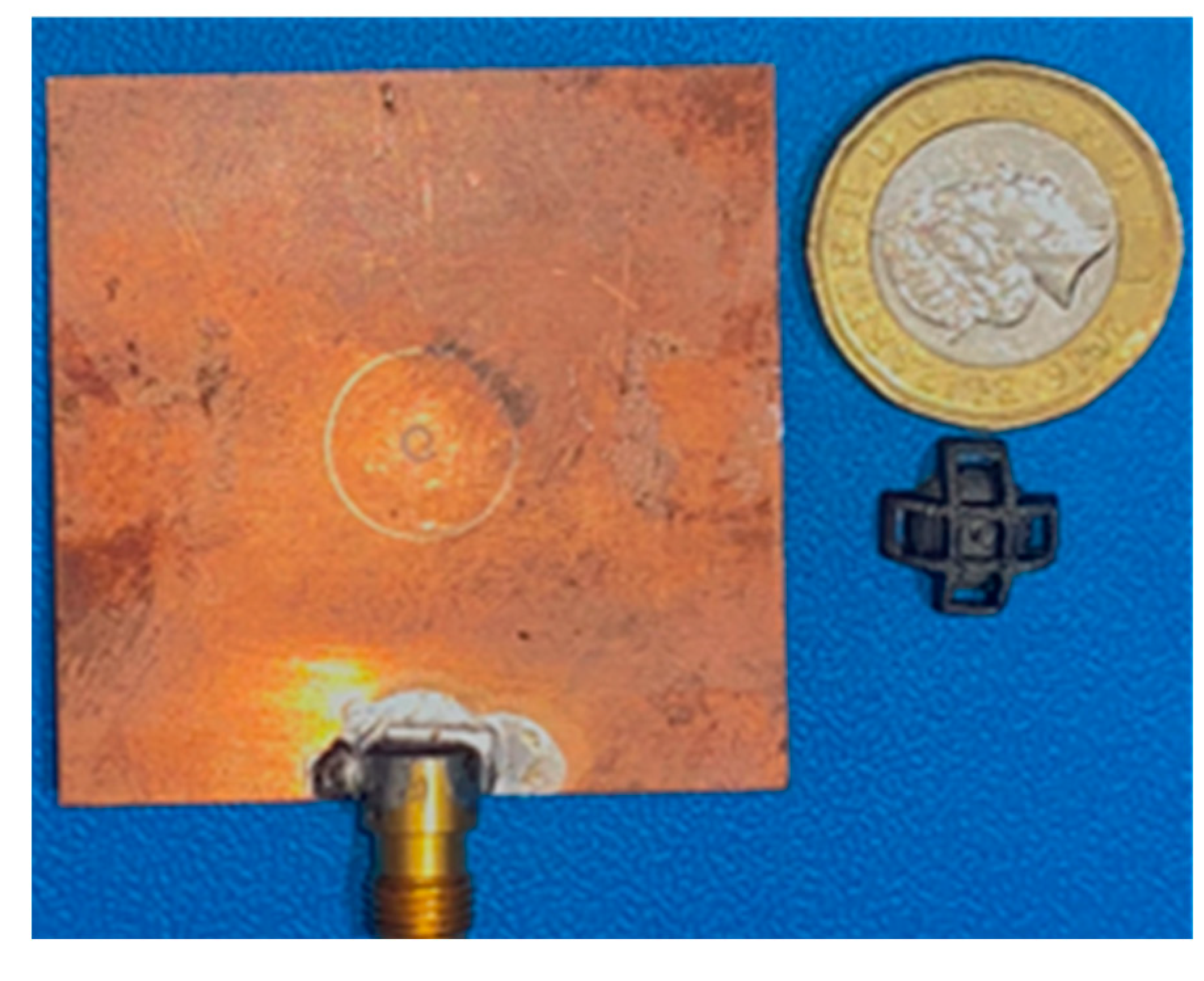
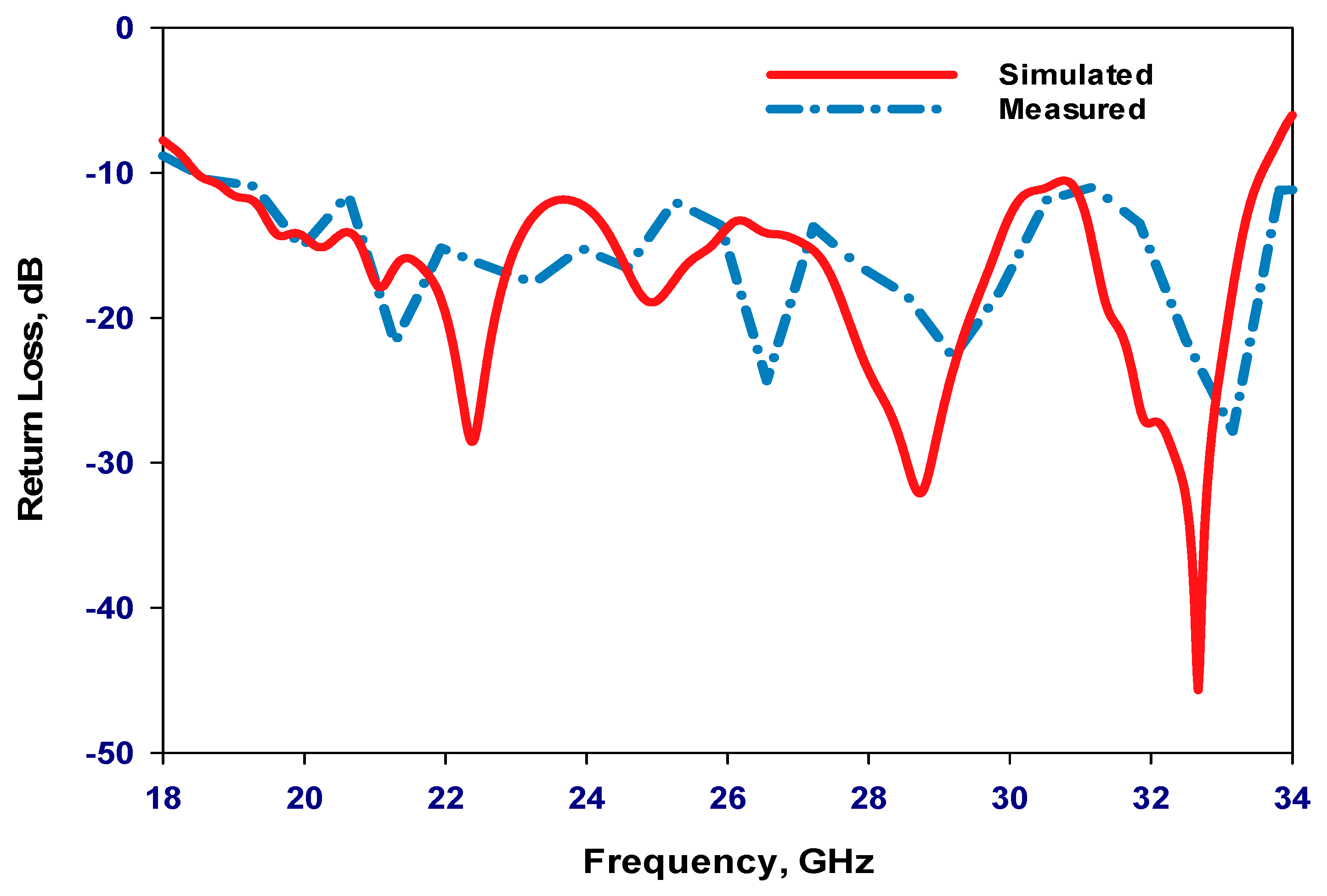
Figure 19 showcases a prototype of the proposed 3D-printed HDRA with a perforated coat. The antenna was built by a 3D mattress company in its final configuration, utilizing a material with a dielectric constant of 10. The same feeding network as previously described was employed. As depicted in Figure 20, measured and simulated results exhibit agreement with respective impedance bandwidths of 59.5% and 58% over frequency ranges of 18.4 to 34 GHz and 18.4 to 33.5 GHz, respectively.
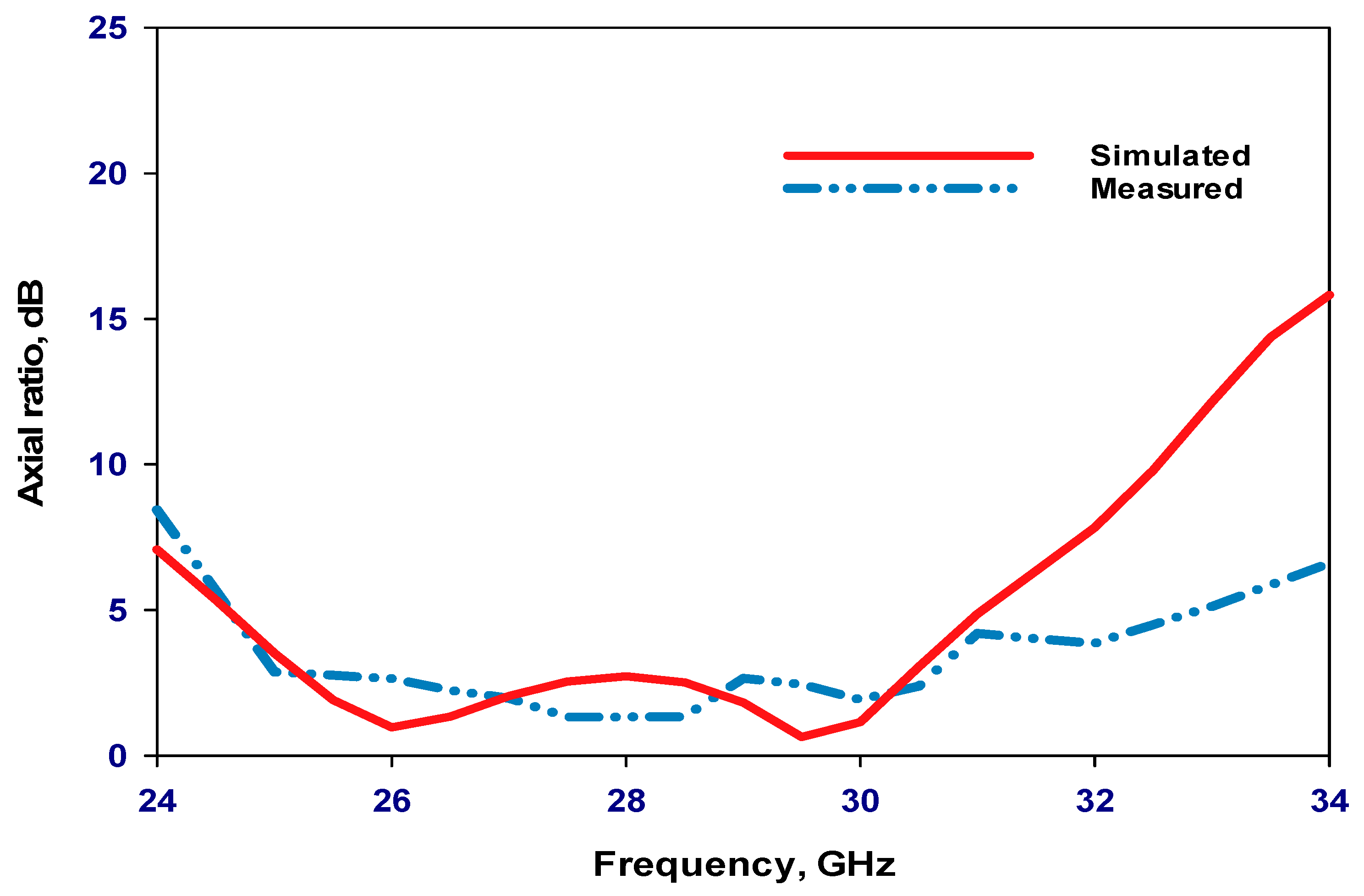
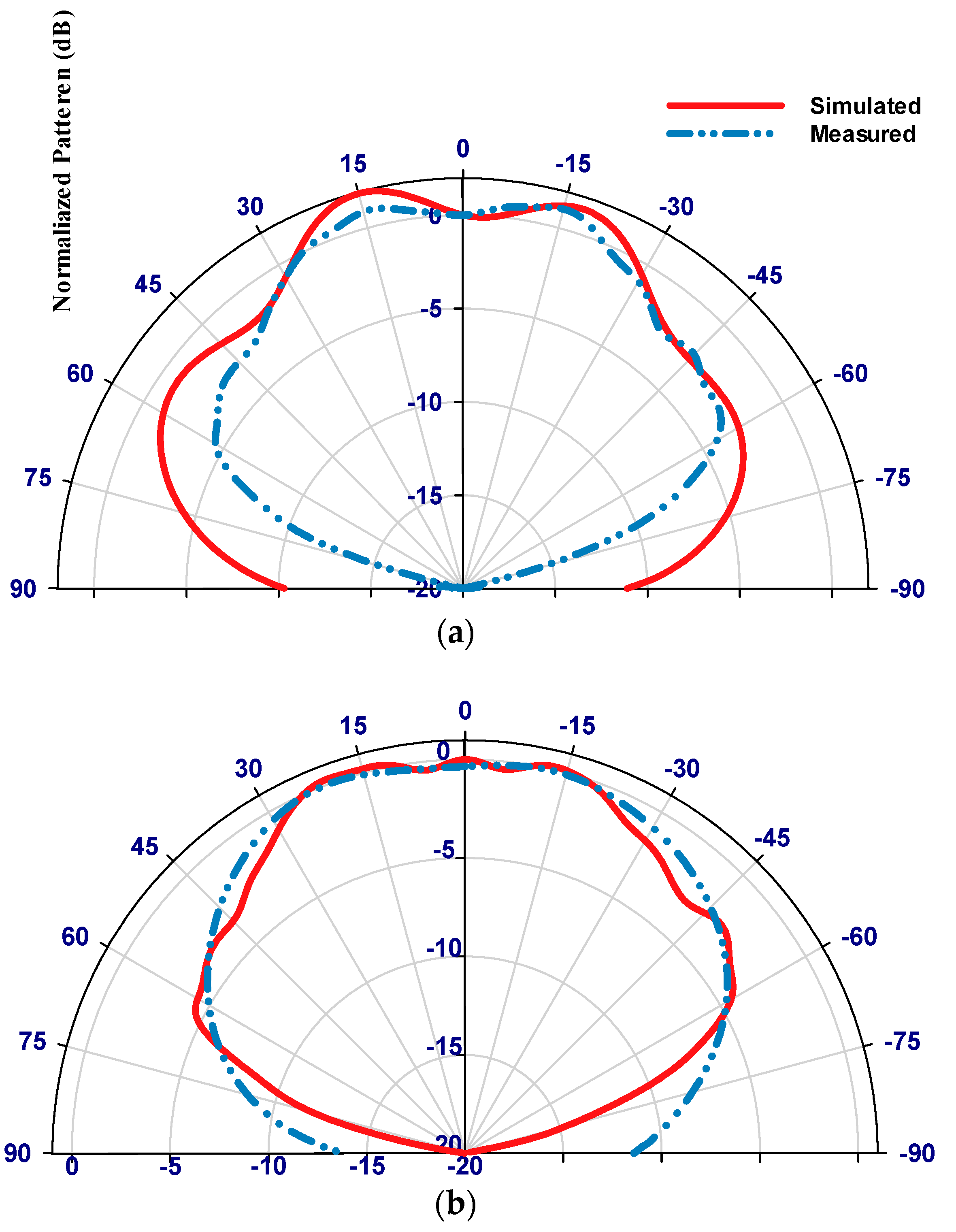
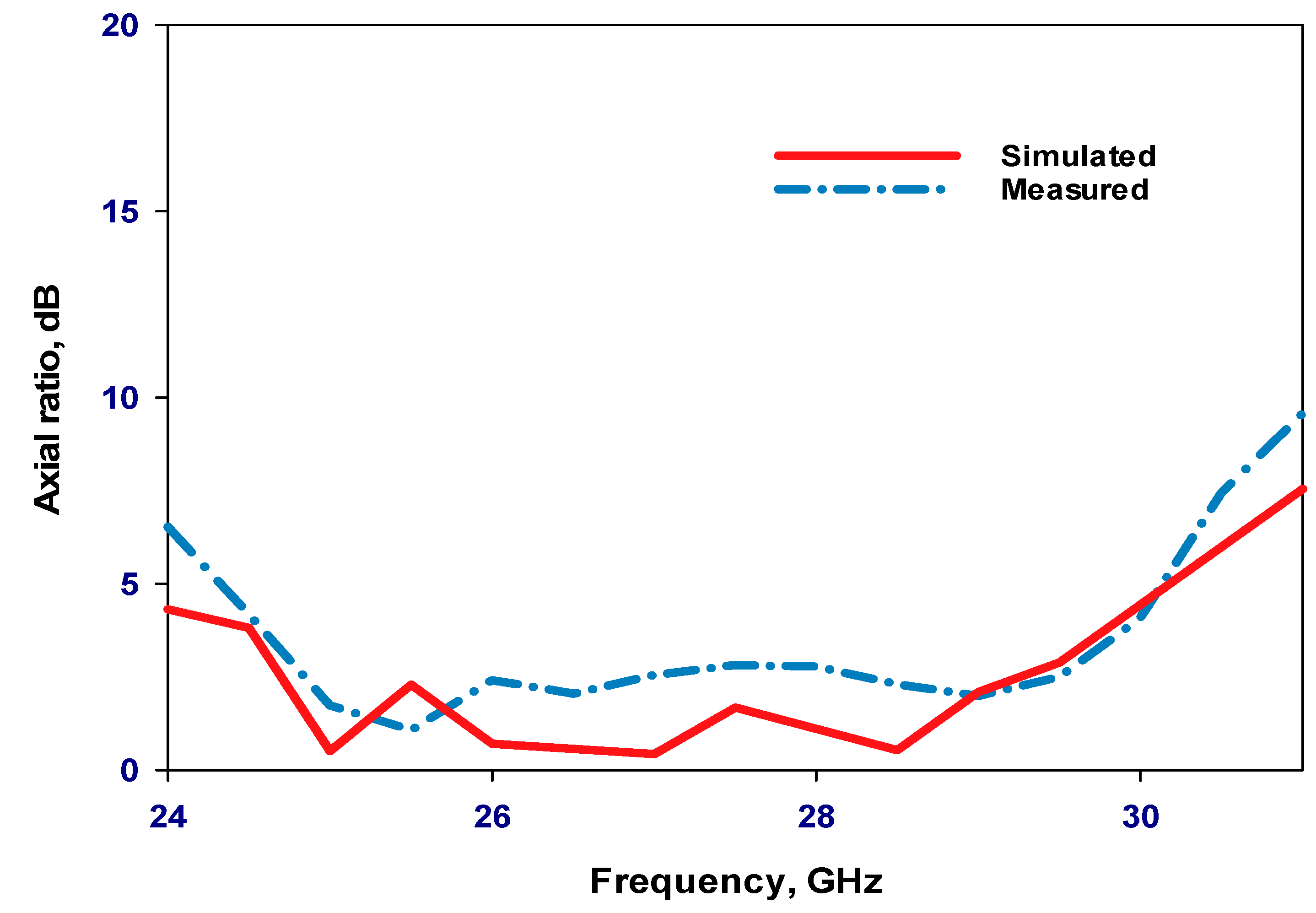
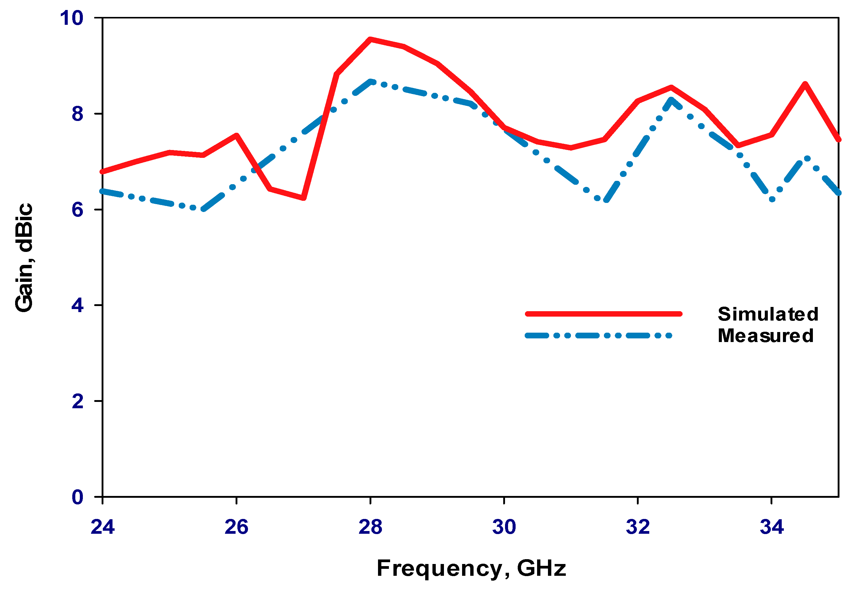
In Figure 21, the measured and simulated AR are presented with respective wide bandwidths of 17.7% and 18%, covering frequency ranges of 24.74 to 29.66 GHz and 24.7 to 29.5 GHz, respectively. As demonstrated in Figure 22, a maximum gain has been achieved at 28 GHz with simulated and measured values of 9.53 dBic and 8.6 dBic, respectively, illustrating the enhanced gain due to the excitation of the higher-order resonance mode of TE511. Figure 23 illustrates a good agreement between simulated and measured H-plane and E-plane radiation patterns at 28 GHz.
Table 1 illustrates a comparative analysis of the performance of the proposed 3D-printed HDRA and those reported in earlier studies. The analysis highlights the distinctive features of the presented 3D-printed HDRA, notably its utilization of a single material of modified alumina sectors, effectively emulating the performance of configurations employing two dielectric layers, which is a departure from the multi-layer approach adopted in previous designs. Key attributes of the proposed HDRA include its capability to generate wide-band circularly polarized radiation, achieving significantly higher gain while maintaining a more streamlined architectural design.
Compared to the references [6,9,11,12,13,15,16,19], the proposed configuration presents a wider impedance bandwidth of 58%. This is slightly narrower than the bandwidths reported in [10,14], which utilized probe feeding and three dielectric layers, potentially posing challenges for mmWave applications. Moreover, the proposed antenna offers superior gain and axial ratio bandwidth performance compared to its reported counterparts. Additionally, it simplifies both the fabrication and assembly processes, potentially reducing production costs and enhancing overall efficiency. These attributes collectively position the proposed design as promising for various wireless communication systems and applications.
4. Conclusions
This study presented a theoretical and practical exploration of a layered hemispherical DRA emitting circular polarization, which is stimulated by a spiral slot feed within the millimeter-wave frequency range. Results demonstrate that incorporating a dielectric coat enhances impedance and axial ratio bandwidths while also boosting gain. This improvement stems from exciting multiple resonance modes beyond the initial dual modes of a single-layer HDRA. Specifically, two-layer HDRA configurations exhibit increased impedance and AR bandwidths of 57% and 18.15%, respectively, coupled with an enhanced gain of 7.5 dBic. Moreover, the successful construction and agreement between simulated and measured results of a two-solid layer HDRA prototype were achieved.
Furthermore, it was demonstrated that an alumina HDRA with a perforated coat can be fabricated via MDF 3D printing, consolidating the two layers into a physical single layer. This streamlines automated assembly and bonding of the layered DRA, eliminating potential air gaps between dielectric layers. This engineered alumina structure, featuring a solid DRA core and a coat characterized by varied air-filling ratios, is designed to achieve the necessary effective dielectric constants. The implementation of an HDRA with a perforated dielectric coat revealed a significant correlation between the two configurations. Additionally, the 3D-printed model exhibited close agreement between simulated and measured results, with impedance bandwidths covering 59.5% and 58%, and CP bandwidths spanning 18% and 17.7%, respectively, within the frequency range of 24.74 to 29.66 GHz and 24.7 to 29.5 GHz. At 28 GHz, simulated and measured gains were 9.53 dBic and 8.6 dBic, respectively.
Considering these attributes, the proposed antenna proves suitable for millimeter-wave satellite communication and radar systems. Furthermore, the superiority of the 3D-printed configuration over its two-solid layers counterpart becomes more pronounced at higher frequencies, such as 60 GHz and sub-terahertz, owing to automated bonding and assembly processes.
Author Contributions
W.A.: conceptional design, simulation, measurements, writing; R.A.: investigation and writing; Y.K.: expertise; S.K.K.: supervision and writing. All authors have read and agreed to the published version of the manuscript.
Funding
This research received no external funding.
Data Availability Statement
Data are contained within the article.
Acknowledgments
The authors would like to acknowledge the use of the National mmWave Facility.
Conflicts of Interest
The authors declare no conflicts of interest.
References
- Petosa, A.; Thirakoune, S. Design of a 60 GHz dielectric resonator antenna with enhanced gain. In Proceedings of the 2010 IEEE Antennas and Propagation Society International Symposium, Toronto, ON, Canada, 11–17 July 2010; pp. 1–4. [Google Scholar]
- Nor, N.M.; Jamaluddin, M.H.; Kamarudin, M.R.; Khalily, M. Rectangular dielectric resonator antenna array for 28 GHz applications. Prog. Electromagn. Res. 2016, 63, 53–61. [Google Scholar] [CrossRef]
- Petosa, A.; Thirakoune, S. Rectangular dielectric resonator antennas with enhanced gain. IEEE Trans. Antennas Propagat. 2011, 59, 1385–1389. [Google Scholar] [CrossRef]
- Gangwar, H.R.K.; Singh, S.; Kumar, D. Comparative studies of rectangular dielectric resonator antenna with probe and microstrip line feeds. Arch. Appl. Sci. Res. 2010, 2, 1–10. [Google Scholar]
- Ng, H.K.; Leung, K. Circular-polarized hemispherical dielectric resonator antenna excited by dual conformal-strip. In Proceedings of the IEEE Antennas and Propagation Society International Symposium (IEEE Cat. No. 02CH37313), San Antonio, TX, USA, 16–21 June 2002; Volume 3, pp. 442–445. [Google Scholar]
- Chen, N.; Su, H.; Wong, K.; Leung, K. Analysis of a broadband slot-coupled dielectric-coated hemispherical dielectric resonator antenna. Microwave Opt. Tech. Lett. 1995, 8, 15–18. [Google Scholar] [CrossRef]
- Abdulmajid, A.A.; Khamas, S. Higher order mode layered cylindrical dielectric resonator antenna. Prog. Electromagn. Res. 2019, 90, 65–77. [Google Scholar] [CrossRef]
- Abdulmajid, A.A.; Khalil, Y.; Khamas, S. Higher-Order-mode circularly polarized two-layer rectangular dielectric resonator antenna. IEEE Antennas Wirel. Propagat. Lett. 2018, 17, 1114–1117. [Google Scholar] [CrossRef]
- Leung, K.W.; So, K.K. Theory and experiment of the wideband two-layer hemispherical dielectric resonator antenna. IEEE Trans. on Antennas and Propagat. 2009, 57, 1280–1284. [Google Scholar] [CrossRef]
- Kakade, A.B.; Ghosh, B. Mode excitation in the coaxial probe coupled three-layer hemispherical dielectric resonator antenna. IEEE Trans. Antennas Propagat. 2011, 59, 4463–4469. [Google Scholar] [CrossRef]
- Kakade, A.; Ghosh, B. Analysis of the rectangular waveguide slot coupled multilayer hemispherical dielectric resonator antenna. IET Microw. Antennas Propagat. 2012, 6, 338–347. [Google Scholar] [CrossRef]
- Kakade, B.; Kumbhar, M. Wideband circularly polarized conformal strip fed three layer hemispherical dielectric resonator antenna with parasitic patch. Microwave Opt. Technol. Lett. 2014, 56, 72–77. [Google Scholar] [CrossRef]
- Abdulmajid, A.A.; Khamas, S.; Zhang, S. Wideband High-gain millimetre-wave three-layer hemispherical dielectric resonator antenna. Prog. Electromagn. Res. C 2020, 103, 225–236. [Google Scholar] [CrossRef]
- Przepiorowski, J.; Munina, I.; Ammann, M.J.; Trimble, D. Fully 3D-Printed Hemispherical Dielectric Resonator Antenna for C-band Applications. In Proceedings of the 2023 17th European Conference on Antennas and Propagation (EuCAP), Florence, Italy, 26–31 March 2023; pp. 1–4. [Google Scholar] [CrossRef]
- Yang, C.; Xiao, Y.; Leung, K.W. A 3D-Printed Wideband Multilayered Cylindrical Dielectric Resonator Antenna With Air Layers. In Proceedings of the 2020 IEEE Asia-Pacific Microwave Conference (APMC), Hong Kong, 8–11 December 2020; pp. 561–563. [Google Scholar] [CrossRef]
- Ghosh, B.; Kakade, A.B. Mode excitation in the microstrip slot-coupled three-layer hemispherical dielectric resonator antenna. IET Microw. Antennas Propagat. 2016, 10, 1534–1540. [Google Scholar] [CrossRef]
- Fang, X.S.; Leung, K.W. Design of wideband omnidirectional two-layer transparent hemispherical dielectric resonator antenna. IEEE Trans. Antennas Propagat. 2014, 62, 5353–5357. [Google Scholar] [CrossRef]
- Xia, Z.-X.; Leung, K.W.; Lu, K. 3-D-printed wideband multi-ring dielectric resonator antenna. IEEE Antennas Wirel. Propagat. Lett. 2019, 18, 2110–2114. [Google Scholar] [CrossRef]
- Albakosh, W.; Asfour, R.; Abdou, T.S.; Khalil, Y.; Khamas, S.K. Wideband Millimeter-Wave Perforated Cylindrical Dielectric Resonator Antenna Configuration. Magnetism 2024, 4, 73–90. [Google Scholar] [CrossRef]
- Xia, Z.-X.; Leung, K.W.; Gu, P.; Chen, R. 3-D printed wideband high-efficiency dual-frequency antenna for vehicular communications. IEEE Trans. Vehic. Technol. 2022, 71, 3457–3469. [Google Scholar] [CrossRef]
- McAllister, M.; Long, S.A. Resonant hemispherical dielectric antenna. Electron. Lett. 1984, 20, 657–659. [Google Scholar] [CrossRef]
- Sarkar, G.A.; Ballav, S.; Chatterjee, A.; Ranjit, S.; Parui, S.K. Four element MIMO DRA with high isolation for WLAN applications. Prog. Electromagn. Res. Lett. 2019, 84, 99–106. [Google Scholar] [CrossRef]
- Qian, Z.; Leung, K.W.; Chen, R.S. Analysis of circularly polarized dielectric resonator antenna excited by a spiral slot. Prog. Electromagn. Res. 2004, 47, 111–121. [Google Scholar] [CrossRef]
- Khamas, S.K.; Starke, P.L.; Cook, G.G. Design of a printed spiral antenna with a dielectric superstrate using an efficient curved segment moment method with optimization using marginal distributions. IEE Proc.-Microw. Antennas Propag. 2004, 151, 315–320. [Google Scholar] [CrossRef]
- Liang, M.; Ng, W.-R.; Chang, K.; Gbele, K.; Gehm, M.E.; Xin, H. A 3-D Luneburg lens antenna fabricated by polymer jetting rapid prototyping. IEEE Trans. Antennas Propag. 2014, 62, 1799–1807. [Google Scholar] [CrossRef]
- UKRI National Millimetre Wave Facility. Available online: https://www.sheffield.ac.uk/mm-wave/ (accessed on 9 March 2024).
Figure 1.
The configuration of the proposed layered HDRA.

Figure 2.
A single-arm feeding spiral slot.

Figure 3.
Simulated return losses of a single layer HDRA.

Figure 4.
Simulated return losses with various radii of the outer layer.

Figure 5.
Simulated axial ratio with various radii of the outer layer.

Figure 6.
Simulated gain with various radii of the outer layer.

Figure 7.
Maximum bandwidth as a function of the outer layer thickness.

Figure 8.
Hemispherical alumina DRA with a perforated alumina dielectric coat.

Figure 9.
The configuration of the hemispherical DRA with a perforated dielectric coat and a feed network.
Figure 9.
The configuration of the hemispherical DRA with a perforated dielectric coat and a feed network.

Figure 10.
Simulated return losses with various unit cell’s wall thicknesses (tc).

Figure 11.
Simulated axial ratio with various wall thicknesses (tc).

Figure 12.
Simulated gain with various wall thickness (tc).

Figure 13.
Simulated return losses of layered HDRA with solid and perforated coats.

Figure 14.
(a) Prototype of the multi-layer hemispherical DRA, and (b) measurements setup.

Figure 15.
The simulated and measured return losses of two-layer HDRA.

Figure 16.
The simulated and measured axial ratio of a layered HDRA.

Figure 17.
Simulated and measured gain of a layered HDRA.

Figure 18.
Simulated and measured of the radiation patterns of a layered HDRA at 28 GHz; (a) ϕ = 0°, (b) ϕ = 90°.
Figure 18.
Simulated and measured of the radiation patterns of a layered HDRA at 28 GHz; (a) ϕ = 0°, (b) ϕ = 90°.

Figure 19.
The prototype of the proposed hemispherical DRA with a perforated dielectric coat.

Figure 20.
The simulated and measured reflection coefficient of an HDRA with a perforated coat.

Figure 21.
The simulated and measured axial ratio of an HDRA with a perforated coat.

Figure 22.
Simulated and measured the gain of an HDRA with a perforated coat.

Figure 23.
The simulated and measured radiation patterns of an HDRA with a perforated coat at 28 GHz. (a) ϕ = 00, (b) ϕ = 900.
Figure 23.
The simulated and measured radiation patterns of an HDRA with a perforated coat at 28 GHz. (a) ϕ = 00, (b) ϕ = 900.


Table 1.
Performance comparison of multi-layered hemispherical DRAs.
| Ref. | Antenna Type | Solid Layers | Feeding Mechanism | |S11| Bandwidth | Gain | AR Bandwidth |
|---|---|---|---|---|---|---|
| [6] | HDRA | 3 | Cross Slot | 35.8% | 9.5 dBi | - |
| [9] | HDRA | 2 | Annular Slot | 55% | - | - |
| [10] | HDRA | 3 | Probe | 65% | 3.5 dBi | - |
| [11] | HDRA | 3 | Waveguide | 9.6% | 6.4 dBi | - |
| [12] | HDRA | 3 | Conformal strip | 34% | - | 4.39% |
| [13] | CDRA | 3 | Probe | 12.2% | 4.69 dBi | 12.6% |
| [14] | HDRA | 3 | Probe | 65.7% | 2.3 dBi | - |
| [15] | HDRA | 3 | Probe | 29% | 4.4 dBi | - |
| [16] | HDRA | 2 | Probe | 32% | 2.5 dBi | - |
| [19] | CDRA | 1 | Cross Slot | 53.3% | 13 dBic | 17% |
| This work | HDRA | 1 | Spiral Slot | 58% | 9.53 dBic | 17.7% |
Disclaimer/Publisher’s Note: The statements, opinions and data contained in all publications are solely those of the individual author(s) and contributor(s) and not of MDPI and/or the editor(s). MDPI and/or the editor(s) disclaim responsibility for any injury to people or property resulting from any ideas, methods, instructions or products referred to in the content. |
© 2024 by the authors. Licensee MDPI, Basel, Switzerland. This article is an open access article distributed under the terms and conditions of the Creative Commons Attribution (CC BY) license (https://creativecommons.org/licenses/by/4.0/).
Share and Cite
MDPI and ACS Style
Albakosh, W.; Asfour, R.; Khalil, Y.; Khamas, S.K. Wideband Millimeter-Wave Perforated Hemispherical Dielectric Resonator Antenna. Electronics 2024, 13, 1694. https://0-doi-org.brum.beds.ac.uk/10.3390/electronics13091694
AMA Style
Albakosh W, Asfour R, Khalil Y, Khamas SK. Wideband Millimeter-Wave Perforated Hemispherical Dielectric Resonator Antenna. Electronics. 2024; 13(9):1694. https://0-doi-org.brum.beds.ac.uk/10.3390/electronics13091694
Chicago/Turabian StyleAlbakosh, Waled, Rawad Asfour, Yas Khalil, and Salam K. Khamas. 2024. "Wideband Millimeter-Wave Perforated Hemispherical Dielectric Resonator Antenna" Electronics 13, no. 9: 1694. https://0-doi-org.brum.beds.ac.uk/10.3390/electronics13091694
Note that from the first issue of 2016, this journal uses article numbers instead of page numbers. See further details here.