Article

Design and Implementation of Reconfigurable Array Adaptive Optoelectronic Hybrid Interconnect Shunting Network

1
School of Electronics and Information, Northwestern Polytechnical University, Xi’an 710129, China
2
School of Electronic Engineering, Xi’an University of Posts &Telecommunications, Xi’an 710121, China
*
Authors to whom correspondence should be addressed.
Submission received: 13 March 2024 / Revised: 15 April 2024 / Accepted: 16 April 2024 / Published: 26 April 2024
(This article belongs to the Special Issue Configurable Computing Systems for Enhanced Industrial Communication)

Abstract

:
Addressing challenges regarding Hybrid Optoelectronic Network-on-Chip systems, such as congestion control, their limited adaptability, and their inability to facilitate optoelectronic co-simulation, this study introduces an adaptive hybrid optoelectronic interconnection shunt structure tailored for reconfigurable array processors. Within this framework, an adaptive shunt routing algorithm and a low-loss non-blocking five-port optical router are developed. Furthermore, an adaptive hybrid optoelectronic interconnection simulation model and a performance statistical model, established using SystemVerilog and Verilog, complement these designs. The experimental results showcase promising enhancements: the designed routing algorithm demonstrates an average 17.5% improvement in mitigating congestion at network edge nodes; substantial reductions in the required number of cross waveguides and micro-ring resonators for optical routers lead to an average path insertion loss of only 0.522 dB. Moreover, the hybrid optoelectronic interconnection performance statistical model supports the design of routing strategies and topology structures, enabling resource usage, power consumption, insertion loss, and other performance metrics to be accurately assessed.

1. Introduction

The burgeoning silicon photonics industry has made the optoelectronic hybrid interconnect structure a pivotal technology in overcoming on-chip communication and storage bottlenecks [1,2]. Yet, existing structures lack adaptability for chip-scale expansion and struggle with the long-distance transmission of varied traffic data, prompting an urgent need for research into adaptive optoelectronic hybrid interconnections tailored for reconfigurable architectures [3,4,5].
In the 2D mesh reconfigurable on-chip network detailed by Oveis et al., comprising communication and router layers, scalability and fault tolerance were limited despite the ability to reconstruct different topological forms [6]. Congestion diversion and obstacle avoidance remain unaddressed. Shan et al. introduced a dynamic self-reconfiguration mechanism, utilizing an H-tree-type interconnection network to enhance performance by enabling the concurrent execution of multiple applications while minimizing context switching time [7].
The 2DMesh-HMRPD(hybrid of mesh-ring with partial diagonal link) hybrid topology proposed by Seetharaman et al. for neuromorphic structures utilizes an optical bus for long-distance, low-latency data communication [8]. However, its complex network structure poses design challenges. Cheng et al. presented the Poet-Opto-Opto-Hybrid Interconnect, which supports low-latency, high-bandwidth communication through an improved optical bus but suffers from poor scalability and throughput under high-traffic conditions [9].
In reconfigurable arrays, effective data interaction among processing elements relies on a routing network formed by interconnecting electrical and optical routers. Parane et al. proposed an adaptive, cost-effective router structure that ensures high reliability under congestion by influencing crossbars, routing algorithms, and router pipeline optimization [10]. Nevertheless, the use of cache bypasses and multiplexers increases hardware overhead and power consumption.
Devadhas et al. introduced an adaptive router structure with variable cache depth, dynamically reallocating cache to directions with significant data traffic [11]. However, its limited total cache depth and reconfiguration delay pose constraints. Shafiei et al. proposed an adaptive routing algorithm based on congestion awareness, aiming to detect congestion and faults in adjacent channels [12]. Yet, its need to constantly check adjacent channel congestion leads to significant communication delays.
This paper proposes an adaptive optoelectronic hybrid interconnect shunting network tailored for novel reconfigurable arrays. Introducing a new adaptive offload router and routing algorithm leveraging both optical and electrical interconnection technologies, this work presents high-performance, low-power, and highly reliable routing architecture, algorithms, and switching methods. These enhancements aim to bolster network bandwidth, improve link efficiency, reduce communication delays, and prevent data transmission blockages, ultimately enhancing reconfigurable device performance.
Moreover, this paper presents a low-loss, low-latency transmission solution for global and local communications, catering to uniform and hotspot data transmission modes within clustered structures. Addressing low perception and fault tolerance, this approach mitigates high link power consumption in hot traffic modes, ensuring accurate and low-delay data transmission to destination nodes.

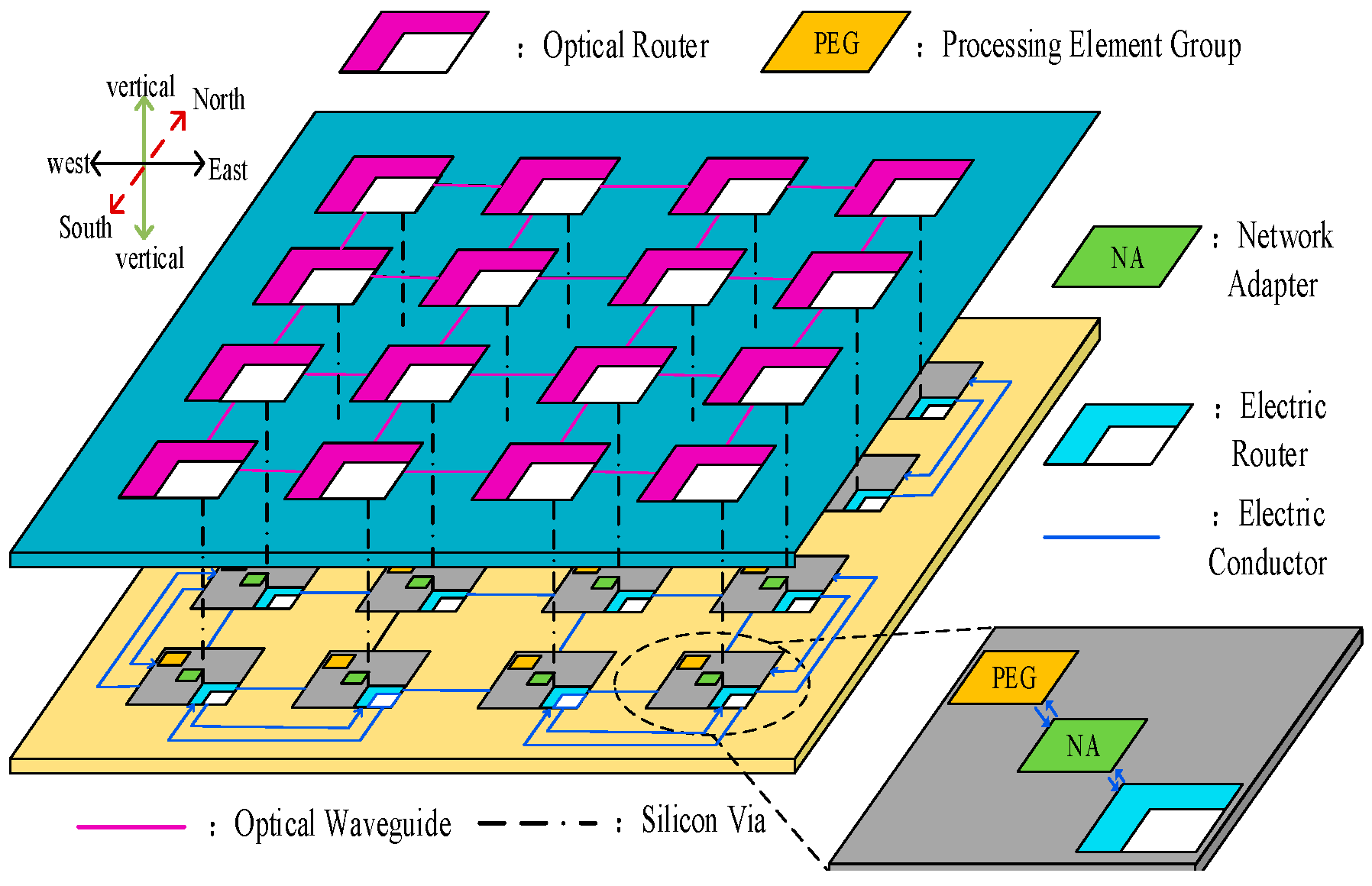
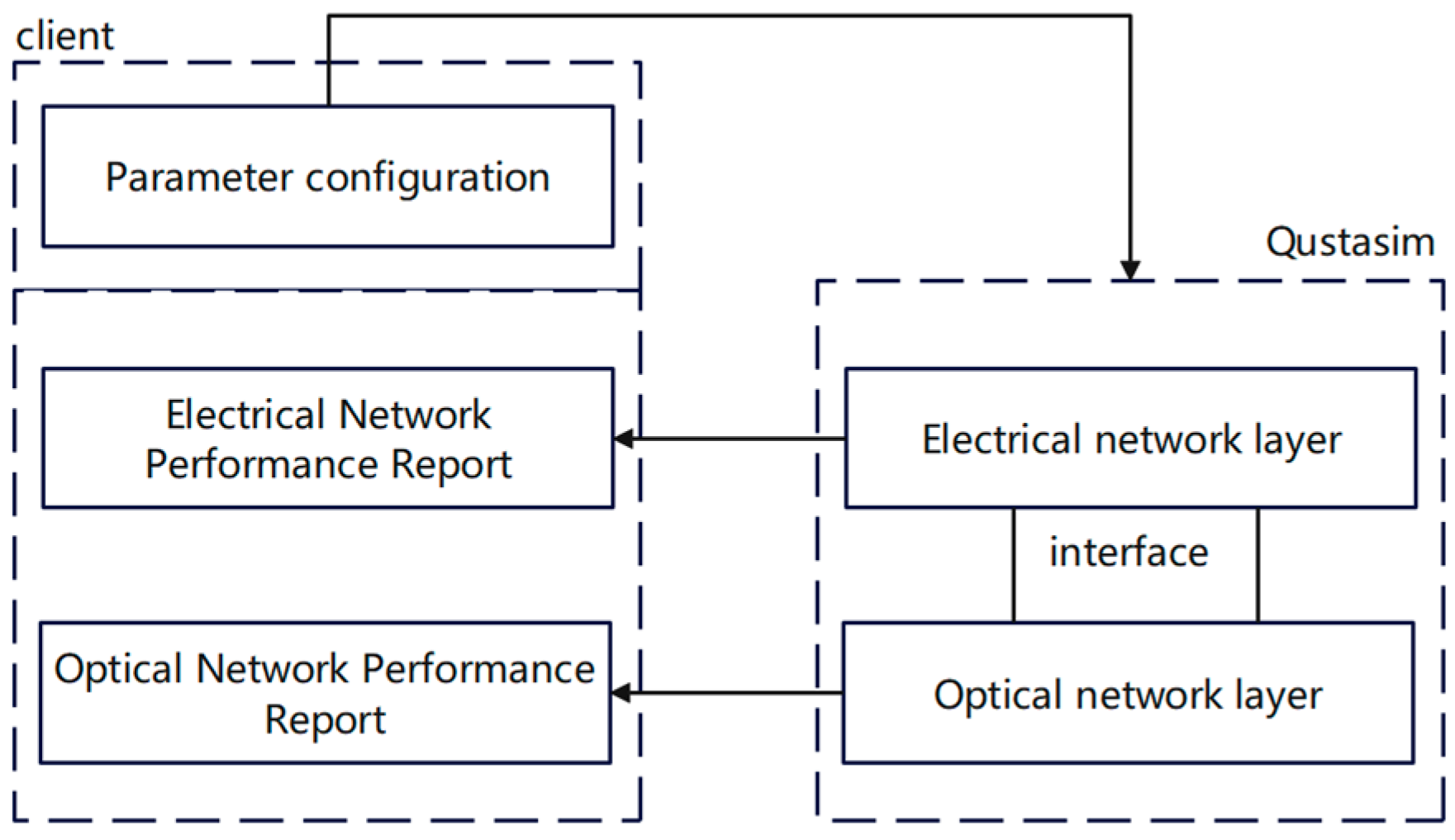
2. Overall Framework of Adaptive Optoelectronic Hybrid Interconnection and Shunting Network

This paper introduces an adaptive optoelectronic hybrid interconnect shunt structure, illustrated in Figure 1, following comprehensive analysis and research on existing reconfigurable array on-chip interconnect structures. The structure comprises a bottom electrical network layer, consisting primarily of a light core Processor Element Group (PEG) [13], a Network Adapter (NA) [14], and an electrical router. Above this layer lies the optical network layer, housing multiple five-port optical routers. The through-silicon via (TSV) [15] cooperative electrical router controls the establishment, response, and termination of optical links between layers, facilitating accurate data communication. Functionally, the electrical router not only manages data circuit exchange but also sends control signals to configure micro-ring resonator states within optical routers. Emphasizing electrical control and optical transmission synergy, this structure optimizes communication resources by connecting unused I/O ports in peripheral routing nodes, effectively distributing data from edge routing nodes within the on-chip network.
Given the frequent communication and data exchange between edge processing element clusters and global controllers or distributed storage modules, these edge nodes often encounter network congestion, uneven load distribution, and reduced network reliability. The proposed offloading structure addresses performance degradation in reconfigurable arrays [16] due to network congestion. The integration of optical networks introduces path diversity, offering multiple alternative communication routes between clusters. This diversity aids in load balancing across the network, even when communication modes are uneven, thereby enhancing overall network reliability.
Delving into the operational intricacies of the adaptive optoelectronic hybrid interconnection shunting network, let us first explore the synergistic functionality of the optoelectronic setup. Figure 2 illustrates the cooperative workings of the optoelectronic structure, delineating three key stages for successful data packet transmission: path establishment, source node response, and link disassembly.
Upon receiving a routing request signal from the processing element cluster, the electrical router initiates path establishment based on the addresses of the source and destination nodes, guided by the adaptive routing algorithm. Once the path is successfully established, the destination node responds by signaling back to the source node. This response triggers configuration adjustments within the micro-ring resonator, aligning its state with the routing path, ensuring coupling with the corresponding layer in the optical network.
Subsequently, upon receiving the response signal, the source node channels the data packet into the optical network layer via the TSV or TSPV(through-silicon photonic via), initiating data transmission following the pre-designed optical router specifications. After the completion of data transmission, the source node transmits link-dismantling information to the destination node, finalizing the release of the optical link.
Furthermore, local IP integration within the optical router involves connecting the photoelectric conversion and electro-optical conversion units, facilitating seamless conversion between electrical and optical signals.

3. Shunt Electrical Interconnect Layer

The topology of the shunt electrical transmission network is shown in Figure 3. In a 4 × 4 mesh network, the outermost I/O ports of edge routing nodes are idle, and 30% of the communication resources are unused. In order to make full use of the limited communication resources in the on-chip network, the idle I/O ports in the peripheral routing nodes of the electric router are connected to realize the data offloading of the edge routing nodes. Figure 3 analyzes the change in data transmission mode after adding path a1 and path d1. From the perspective of PEG00, after adding path a1, two paths, a and a1, can be used when transferring data from PEG10 to PEG00. In the worst case, when data in three directions (Local_IP, north, east) are routed to PEG00 at the same time, paths a and a1 can respond to the transmission of two sets of data at the same time. Similarly, after adding path d1, from the perspective of PEG01, two paths, d and d1, can be used when transferring data from PEG00 to PEG01. It can be seen from this that the newly added path a1 and path d1 have the effect of data distribution. As an optoelectronic hybrid interconnection network, the addition of optical networks has enriched the diversity of the paths. When transmitting data from PEG00 to PEG01, not only two electrical transmission paths, d and d1, can be used, but also an optical transmission network can be used, and data from three directions can be transmitted simultaneously in the worst case. It is only necessary to design a more appropriate routing algorithm to transmit the data to avoid path congestion.

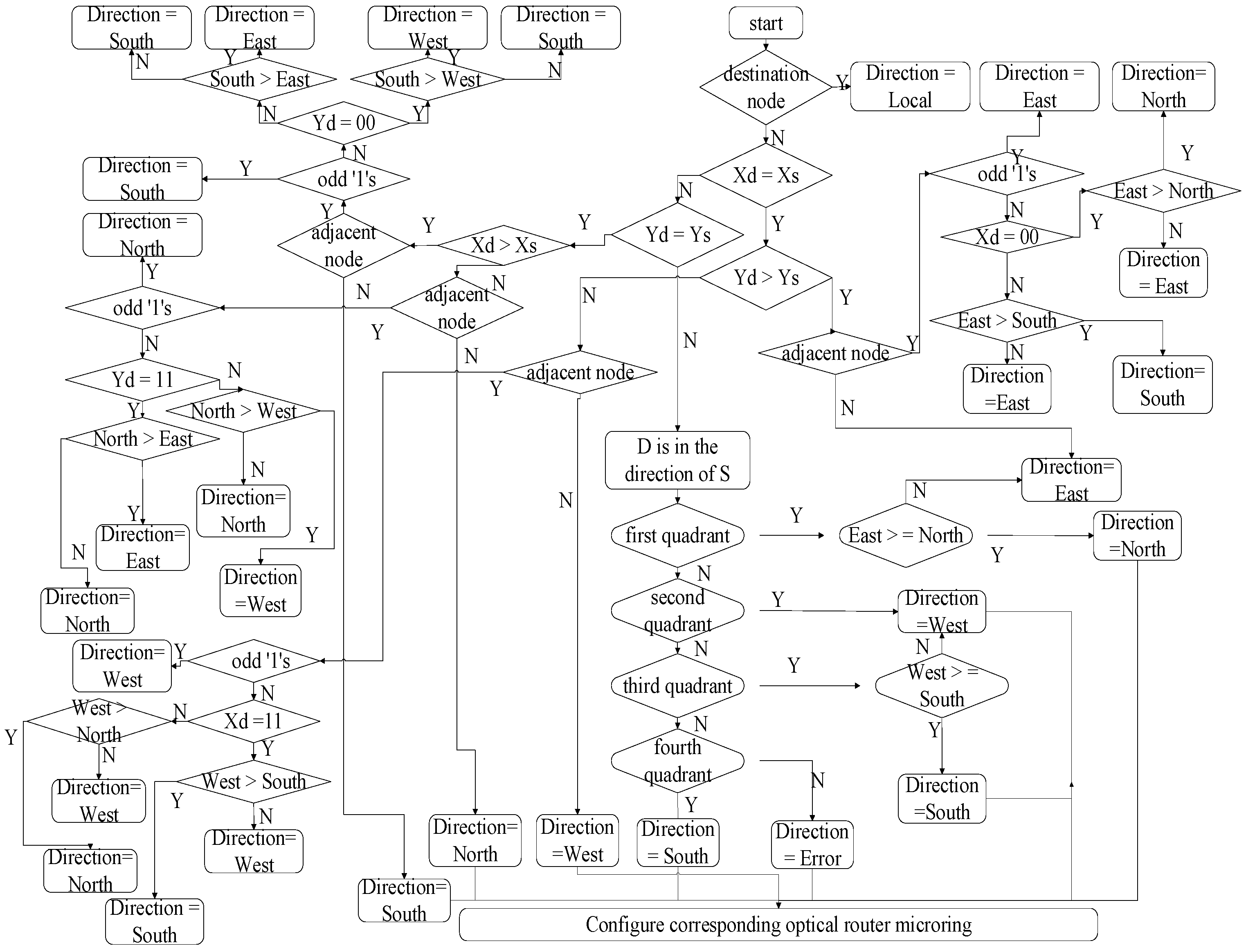
3.1. Routing Algorithm

Frequent optical/electrical conversions can compromise network performance, while the power consumption of electrical interconnections escalates with their length. The Adaptive Streaming Routing Algorithm (ASRA), depicted in Figure 4, enables communication with any node within the network. Adjacent nodes are linked via on-chip electrical interconnections employing circuit switching for communication. In contrast, non-adjacent nodes utilize on-chip optical interconnections and communicate through optical routers.
For instance, when PEG00 transmits data to PEG10, the algorithm assesses whether the X coordinates of the source and destination nodes match. If the X coordinates differ while the Y coordinates align and the X coordinates differ by only 1, signaling adjacent nodes, electrical transmission is chosen. Subsequently, the algorithm evaluates the nodes’ positions: the number of ‘1’s in 4’b0000 is 0, while the number of ‘1’s in 4’b0100 is 1, summing up to an odd number (1). This indicates that there is two available paths between the nodes. Path selection depends on the congestion levels in the west and south directions. If the south port congestion exceeds that in the west port, the algorithm directs output through the additional west port diversion path; otherwise, data are routed through the south port.
Given the higher communication frequency between adjacent clusters, leading to potential electrical network congestion, the adaptive offload routing method offers diverse alternative paths, mitigating data transmission bottlenecks and enhancing overall processor performance.

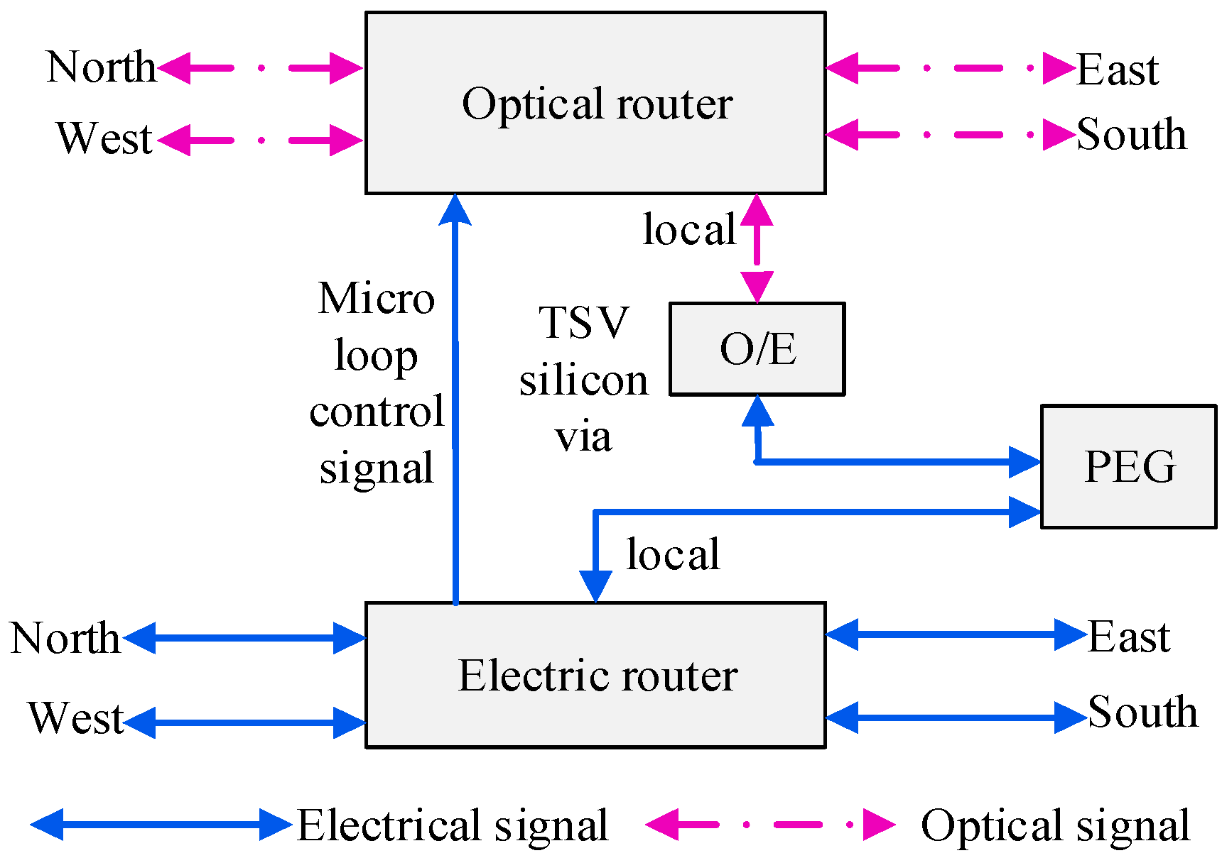
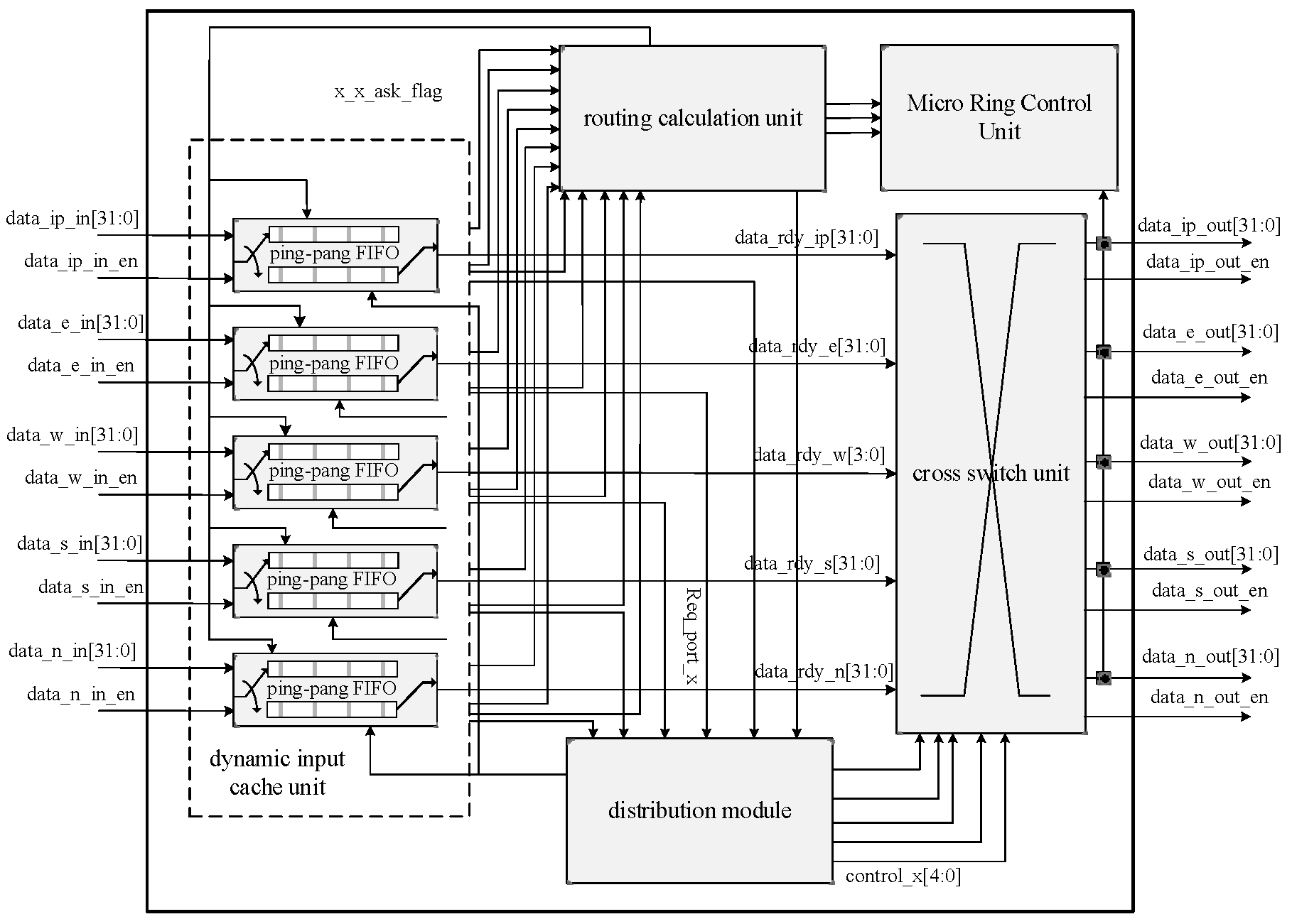
3.2. Electric Router Structure

A robust routing architecture serves as the fundamental cornerstone for the seamless operation of the adaptive shunt network. Figure 5 depicts the structural block diagram of the adaptive shunt electric control router developed in this study. This router primarily consists of a dynamic input buffer unit, a cross-switch and distribution unit, a routing calculation unit, and a micro-ring control unit. Upon the transmission of a routing request signal from the processing meta-cluster, the data packet is placed into the dynamic buffer, awaiting the router’s allocation of the routing path.
The routing calculation unit orchestrates path planning based on the source and destination node positions, current router congestion status, and the adaptive diversion routing algorithm designed by the circuit. Simultaneously, the distribution unit conducts polling and arbitration on the initiating request port, guiding the crossbar to establish connections between input and output ports. Meanwhile, the micro-ring control unit fine-tunes the corresponding micro-ring resonator in the optical network layer to a coupled resonance state, as allocated by the routing calculation unit. This ensures unobstructed data transmission through the waveguide, facilitating smooth delivery to the processing element cluster linked to the destination node address.
Within the electronically controlled router, the dynamic buffer input unit employs a ping-pong buffer structure, enabling simultaneous data writing and routing. The routing calculation unit dynamically selects an optimal transmission path based on network congestion conditions, effectively curbing real-time hotspot occurrences and thereby enhancing the entire reconfigurable array’s performance. The crossbar unit integrates an N-to-one multiplexer, while the distribution unit adopts a polling arbitration mechanism for priority determination. Similarly, the micro-ring control unit adjusts the relevant micro-ring resonator to a coupled state according to the assigned routing path, ensuring unimpeded data transmission through the waveguide.
Moving on to the performance analysis of the shunt router, Table 1 presents a comparison of hardware resource utilization between the offload router designed in this study and the on-chip hybrid router proposed in [17,18,19]. Our router utilizes 65.9% fewer register resources and 65.1% fewer LUT resources than the router in [19]. In comparison to routers mentioned in the literature—EDVC F-R/W, ViChaR, and CDVC—our design reduces register resource utilization by 2.3%, 58.5%, and 0.2%, and LUT resource utilization by 0.3%, 26.7%, and 20.8%, respectively [18]. While our router shows an 11.9% increase in register resource consumption compared to the asynchronous router presented by Patil et al., it exhibits a 2.4% reduction in LUT resource usage [17].
Figure 6a,b depict the throughput variation curves of different routers in both uniform and hotspot traffic modes, where throughput measures the maximum number of received packets by the receiver within a specific timeframe. The results demonstrate that the adaptive split routing structure outperforms the three routers proposed by Fard et al. across both traffic modes [18]. In the uniform mode, at an information injection rate of 0.6, this paper’s routing structure elevates throughput for the CDVC, ViChaR, and EDVC F-R/W routers by 58.8%, 55.8%, and 9.9%, respectively. Similarly, in the hotspot mode, at the same information injection rate, this paper’s routing structure increases throughput for the CDVC, ViChaR, and EDVC F-R/W routers by 87.6%, 22.2%, and 20.4%, respectively. Notably, the routing structure proposed in this paper consistently exhibits higher throughput at equivalent injection rates.
Figure 7a,b illustrate the relationship between information injection rates and average information delay under both uniform and hotspot traffic patterns, comparing our results with those of the shared dynamic cache router proposed by Madsen et al. [20]. The findings demonstrate the superior performance of the adaptive offload routing structure in both traffic modes. In the uniform mode, at an information injection rate of 0.3, this paper’s routing structure reduces average information transmission delays (time data travel from the source to the destination) by 17.3% and 43.4%, respectively, in contrast to the multi-channel dynamic cache router and the multi-channel static router proposed by Madsen [20]. Similarly, in the hotspot mode, at an information injection rate of 0.5, the routing structure proposed in this paper reduces average information transmission delays by 29.2% and 79.1%, respectively, compared to the multi-channel dynamic cache router and the multi-channel static router proposed by Madsen [20]. Remarkably, our proposed routing structure consistently exhibits lower network transmission delays at equivalent injection rates.

3.3. Algorithm Establishment Cycle and Delay Analysis

In situations where the XY Deterministic Routing Algorithm (XY-DRA) [21] encounters blockages, establishing a new link is only feasible after dismantling the existing path. To assess the efficiency of the ASRA, two routing algorithms were compared and analyzed under edge path blockages (specifically, four paths: PEG00-PEG10, PEG02-PEG03, PEG23-PEG33, and PEG30-PEG31). Table 2 records the number of clocks required for the path establishment process and micro-ring configuration process from source node PEG00 to various destination nodes. The findings indicate that the XY-DRA faces high blocking probabilities and extensive path establishment durations, while the ASRA demonstrates the capacity to divert transmissions by monitoring forward path congestion. This diversion mechanism enhances congestion avoidance by an average of 17.5% compared to the XY-DRA. It is worth noting that the router becomes blocked when the port blocking probability reaches 80%.
Figure 8 and Figure 9 present statistical data on the average network delay and throughput derived from the adaptive routing algorithm, the fault-tolerant routing algorithm, the original ant colony algorithm, and the ASRA proposed in this paper across varying injection rates. The findings indicate ASRA’s superior performance compared to the other three algorithms, particularly as the injection rate increases. At injection rates below 0.007, there is minimal disparity in the average network delay among the four algorithms. However, at 0.011 injection rate, significant divergence in network delay between the algorithms becomes evident. At 0.013 injection rate, the ASRA showcases a 35.7% reduction in average delay compared to the adaptive routing algorithm, a 25.6% reduction in average delay compared to the fault-tolerant routing algorithm, and a 7.5% reduction in average delay compared to the original ant colony algorithm. Thus, the ASRA exhibits superior anti-blocking capabilities at equivalent injection rates, minimizing network delay and effectively reducing data wait times.
In terms of average throughput, there is no notable difference among the algorithms at injection rates below 0.17. However, at 0.2 injection rate, the ASRA displays a 7.7% increase in throughput compared to the adaptive routing algorithm and an 8.4% increase compared to the fault-tolerant routing algorithm. Additionally, the ASRA outperforms the swarm algorithm by 16.5% at this rate.
In conclusion, the adaptive optoelectronic hybrid interconnect split routing algorithm developed in this paper exhibits rapid path establishment, minimal data transmission delays, and a high throughput. Notably, it offers three additional turning possibilities compared to the traditional XY routing algorithm. Its versatility allows for effective management across various applications and modes, including non-uniform and burst transmission modes. This algorithm adeptly balances network loads, mitigates congestion, and addresses the limitations typically associated with routing paths.

4. Optical Network Layer

4.1. Optical Network Architecture

Five-port optical routers are used to realize data transmission between different nodes, including local ports (Injection and Ejection), north ports, south ports, west ports and east ports, which are composed of crossbar switches and optical waveguides. As shown in Figure 10, data communication is not performed between ports in the same direction. Micro-ring resonators [23] are not required for wavelength coupling between the two ports directly connected by the waveguide. Micro-ring resonators are used between the remaining ports to perform optical signal transmission direction changes so that the optical signal is transmitted to a fixed destination port. The micro-ring resonators MR1, MR2, MR3, MR4, MR5, and MR8 are multi-angle coupling micro-ring resonators, and one micro-ring resonator can realize the mutual communication between the two groups of ports.
A five-port optical router achieves non-blocking communication among its ports by utilizing five waveguides and ten micro-ring resonators, each with specific assignments, as detailed in Table 3. The communication process unfolds as follows: Ports communicating in the same direction, such as the north port with another north port, directly interact through waveguides without the need for micro-ring resonators to alter transmission direction.
For instance, when the north port communicates with the south port, the signal is transmitted directly through the waveguide without needing a micro-ring resonator for directional changes. However, communication between ports in different directions involves micro-ring resonators to alter signal paths. When the north port communicates with the west port, the signal is initially transmitted from the north port along a waveguide. Upon reaching MR1, the signal undergoes coupling, redirecting it along another waveguide to the west port.
Similar processes occur for communication between the north port and the east port (via MR2) and the Ejection port (via MR8). The communication patterns between other ports mirror these principles, emphasizing no direct communication between ports in the same direction. Ports connected by a waveguide communicate directly without involving micro-ring resonators, whereas communication involving other ports necessitates micro-ring resonance to guide data transmission towards specific ports.

4.2. Performance Analysis of Non-Blocking Five-Port Optical Router

An optical router necessitates various devices, including micro-ring resonators, optical waveguides, curved waveguides, cross waveguides, and optical terminals. The five-port optical router discussed in this study utilizes multi-coupling micro-ring resonator switches. It operates with a single waveguide connecting the input and output of different ports, requiring no optical terminals. In this setup, 10 micro-ring resonators, 9 cross waveguides, and 5 curved waveguides facilitate communication among any port combinations. Table 4 enumerates the optical device count for the five-port optical routers across various references from the literature. Our designed optical router demonstrates efficiency compared to existing models: in comparison to the Rigor optical router, it utilizes only five waveguides, reducing cross waveguides by 25%, curved waveguides by 75%, and micro-ring resonators by 33.3% [22]. In comparison to the Srax optical router, our design reduces cross waveguides by 18.2%, curved waveguides by 54.5%, and micro-ring resonators by 33.3% [24]. Even when compared to [25], while slightly increasing micro-ring resonator usage by two, our design notably reduces cross waveguides by 35.7% and curved waveguides by 80.8%.
The magnitude of insertion loss primarily hinges on the count of micro-ring resonators, curved waveguides, and crossed waveguides within the optical router. Many references in the literature adopt distinct methodologies and parameters for insertion loss calculation. Linsert signifies the insertion loss of different paths. In the literature, the insertion loss value when the micro-ring resonator is not coupled stands at 0.005 dB, denoted as Lthrough, while the coupled micro-ring resonator’s insertion loss registers at 0.5 dB, indicated by Ldrop [22,25]. The crossed waveguide exhibits an insertion loss value of 0.12 dB, referred to as Lcross. Considering the relatively negligible propagation and bending losses in waveguides, they are disregarded in insertion loss analysis. Shi et al. further distinguishes losses of micro-ring resonators into cross-switching and parallel-switching losses [24]. For an equitable comparison, the insertion loss of each path in the optical router aligned with Equation (1), consistent with the referenced literature.
Figure 11 depicts the insertion loss between distinct input and output ports of the five-port optical router devised in this paper. From this analysis, the router’s maximum, minimum, and average insertion loss were determined, detailed in Table 5. Our designed optical router surpasses counterparts of the same category in terms of insertion loss. Compared to optical routers, it showcases a 53.4% and 43.2% reduction in average insertion loss, respectively [22,26]. Although there is a 1.72% increase in insertion loss compared to that of Shi et al., it is worth noting that this increase occurs despite a 33.3% reduction in the number of micro-rings [24].
L insert = N through L through + N drop L drop + N cross L cross

4.3. Development of Optical Network Performance Evaluation Model

To address the existing challenge of unachievable optoelectronic co-simulation, we have developed an adaptive optoelectronic hybrid interconnection function simulation and performance statistical model. This model was crafted using System Verilog and Verilog to construct the optical and electrical networks, including routers, links, channels, and routing policies [27]. It performs statistical analyses on fundamental performance metrics such as resource utilization, power consumption, and insertion loss. Data transmitted via the electrical router are collected through the interface, ensuring accurate data sampling facilitated by the Clocking clock block. Meanwhile, the optical routing network analyzes the interface-collected data to identify source and destination nodes, allocating optimal routing paths for transmission.
Figure 12 is a workflow diagram of the optical network performance evaluation model, which is mainly divided into the user configuration end and the QuestaSim 10.4e operation processing end. First, the network scale, optical router type and different types of waveguide losses on the parameter configuration side are configured. Secondly, the core code is executed on the QuestaSim running processing side to perform statistics on the performance of the optical network and the electrical network. Finally, the statistical results are generated into a visual performance report to facilitate user analysis and statistics.
The performance parameters of the electrical router can be obtained based on the report generated after circuit synthesis. Using the interface to simulate the data interaction from the electrical network layer to the optical network layer can effectively improve the code reuse rate. In addition, the use of the interface can better distinguish electrical routers from optical routers, effectively avoiding data confusion caused by incorrect port input/output direction definitions. When you need to add signals, you only need to declare them once in the interface.
Figure 13 depicts the configuration interface for optical router parameters. This interface allows for the configuration of network scale, optical router type, micro-ring resonator coupling loss, cross waveguide loss, waveguide propagation loss, and waveguide bending loss. Leveraging Qt Creator 5.9, we have developed a graphical interface to generate and store configuration parameters in the ‘config’ configuration file. System Verilog reads this ‘Config’ information to construct an optical routing network. Subsequently, Questasim 10.4e simulator is employed to assess network performance, capturing and presenting performance parameters in a graphical display, as shown in Figure 14. The left side of Figure 14 outlines the data transmission path from the source to the destination node, while the right side exhibits the optical routers used within the network. A comprehensive report detailing network resource usage, power consumption, insertion loss, and other performance metrics is generated for further analysis.

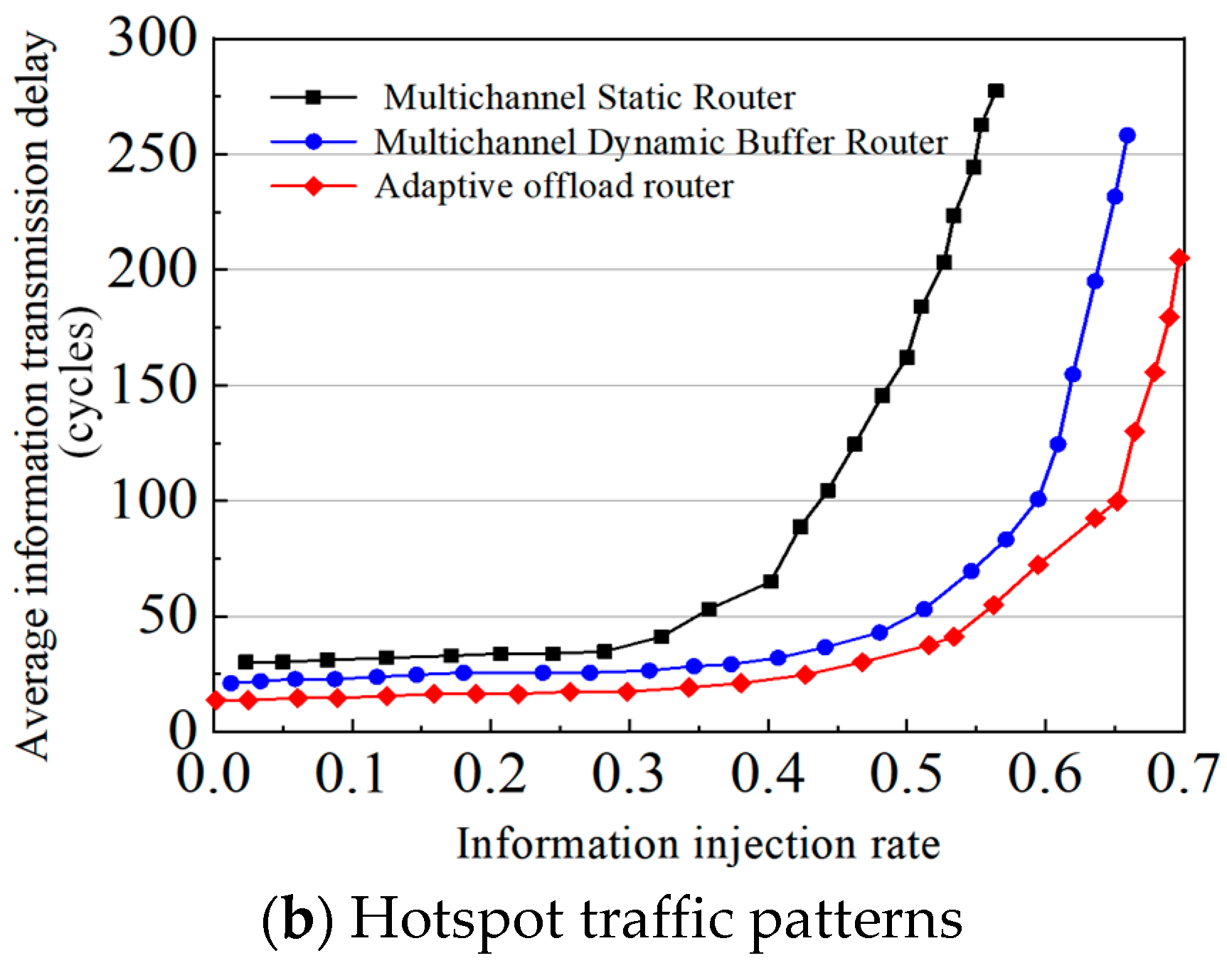
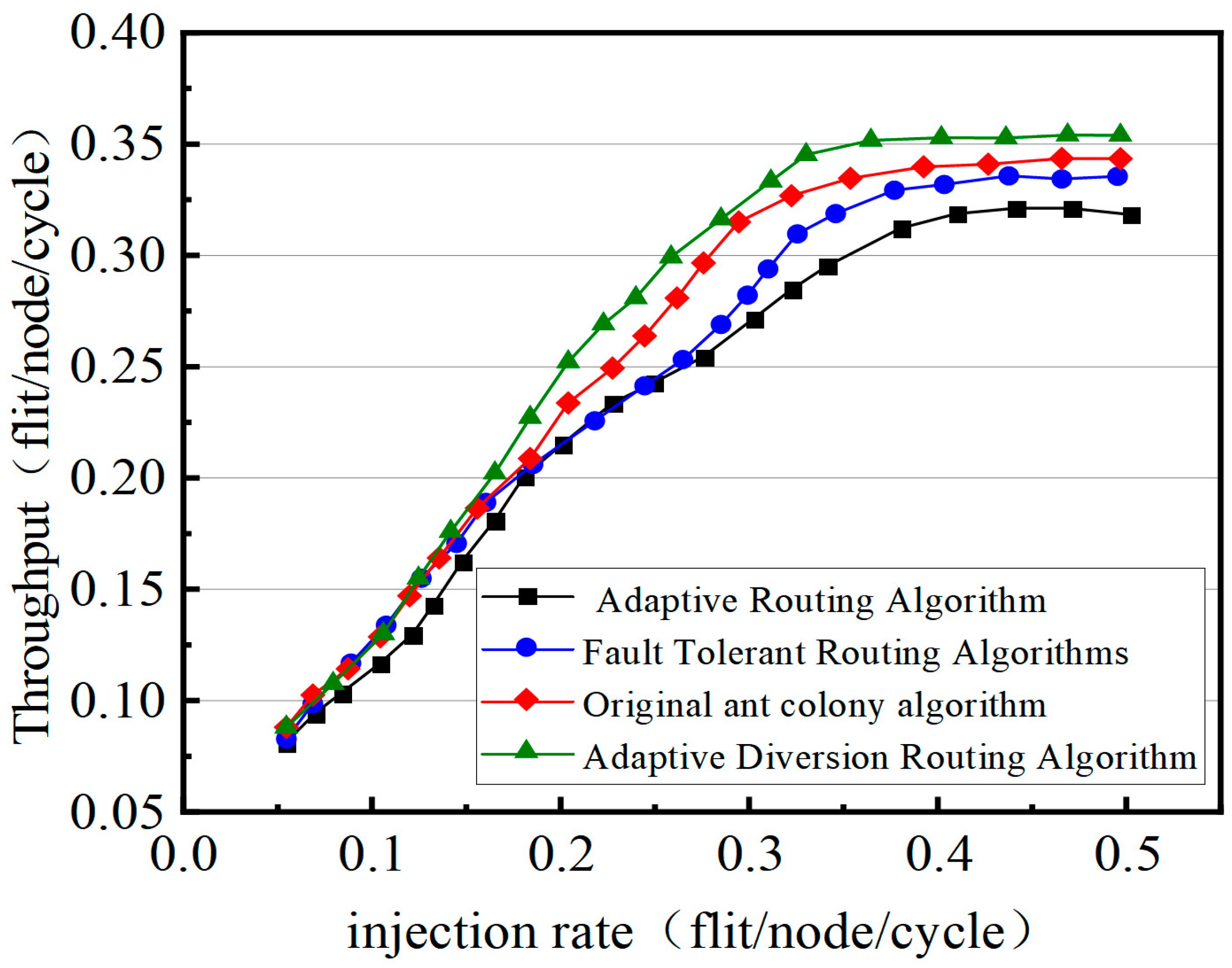
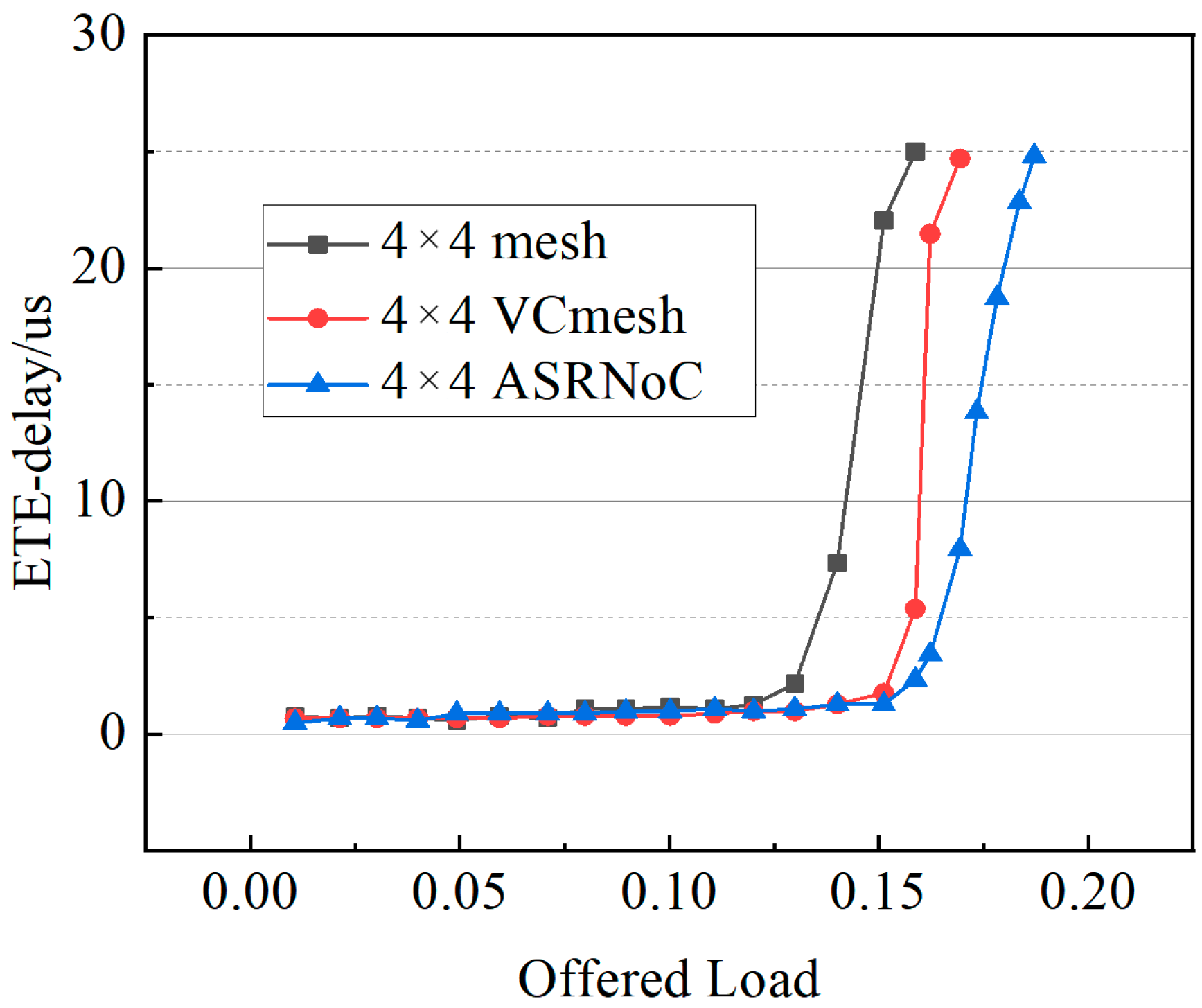
5. Performance Analysis of Shunt Network for Adaptive Optical Hybrid Interconnection

Assessing network performance in adaptive optoelectric hybrid interconnect shunting networks involves crucial metrics like end-to-end (ETE) latency and network throughput (data rate transferred from one point to another). To evaluate these metrics, we employed OMNET++, a discrete event scheduling task-based network simulation software, conducting simulations across varying network scales to obtain diverse latency and throughput results.
Figure 15 and Figure 16 present a comparative analysis of end-to-end delays across different networks of mesh and VCmesh [28] at varying injection rates. The findings demonstrate that the Adaptive Shunt Routing Network-on-Chip (ASRNoC) exhibits notably lower network delays, especially under heavy loads. This advantage stems from the adaptive scheduling of offload expansion paths, showcasing superior performance under increased network traffic.
Figure 17 and Figure 18 present statistical insights into the saturated throughput across various network sizes, considering injected packet sizes of 1024 bits and 4096 bits. In a 5 × 5 network size with a packet injection size of 4096 bits, the throughput of the ASRNoC network surpasses the VC mesh [28] and mesh networks by 4.76% and 28.57%, respectively. These findings underscore the superior throughput performance of ASRNoC compared to the VC mesh [28] and mesh networks described by Su et al. across different scales. ASRNoC showcases higher throughput and reduced network latency in both uniform and hotspot modes owing to its dynamically reconfigurable mechanism.
Network latency in ONoC is the time interval that a packet is transmitted from the source node until it is received by the destination node, which includes transmission latency, configuration latency, and processing latency. We extended the reconfigurable array structure to 4 × 4 and 16 × 16 PEGs, mapped the ASRA algorithm mentioned above, and compared the average latency, which was 14.3% and 23.8% lower than GRPMM [29], much lower than ENoc-XY [29], as shown in Figure 19.
In order to verify the applicability, we tried to map a simplified LeNet network to the array structure of this article and conducted an application test on gesture recognition. When the training number was 1000, the structure of this article was more accurate in recognition than the structures presented in [30,31,32]. The speed reaches the average level, and the speed of recognizing pictures can provide lower recognition time due to the advantages of the network structure, as shown in Figure 20.

6. Conclusions

This study aimed to address the problems of the poor congestion control and self-adaptation ability of optoelectronic hybrid interconnection networks, as well as their inability to realize optoelectronic co-simulation and the characteristics of frequent communication between adjacent processing clusters of reconfigurable array processors. The I/O ports on the periphery of electrical routers are idle. This paper proposes an adaptive optoelectronic hybrid interconnect shunting structure suitable for reconfigurable array processors. Based on this structure, an adaptive shunting routing algorithm and a low-loss and non-blocking 5-port optical router were designed and built based on System Verilog and Verilog. The optoelectronic hybrid interconnection function test and performance statistical model were presented. The experimental results show that the electrical router has a high operating frequency, strong anti-blocking ability, low resource overhead, and low insertion loss. The designed optoelectronic hybrid interconnection network, according to the statistical analysis model used to analyze performance, can accurately judge the network performance of the two transmission modes of hybrid optoelectronics.
This article conducted a data analysis on an on-chip optical-electronic hybrid interconnection network. These types of networks have the following advantages: the routing algorithm enhances the performance of reconfigurable array processors; low-loss, low-overhead optical routers increase transmission rates; and performance models ensure accuracy. Future research might consider applying this network to large-scale multicore processors and AI accelerators, and the same approach could also be extended to data centers and cloud computing. Unfortunately, due to experimental and technological constraints, this paper could not integrate on-chip optical devices into the hybrid network. Considering metasurfaces [33] may be a direction for future research.

Author Contributions

Methodology, B.Y. and R.S.; Software, C.X. and Y.F.; Validation, R.S. and Y.F.; Formal analysis, B.Y., C.X. and Y.F.; Investigation, R.S.; Resources, C.X.; Data curation, Y.L. and J.L.; Writing—original draft, B.Y.; Writing—review & editing, Y.L.; Visualization, B.Y. and J.L.; Supervision, Y.L.; Project administration, Y.L. and J.L. All authors have read and agreed to the published version of the manuscript.

Funding

National Natural Science Foundation of China (No. 61834005).

Data Availability Statement

Data are contained within the article.

Conflicts of Interest

The authors declare no conflict of interest.

References

  1. Atabaki, A.H.; Moazeni, S.; Pavanello, F.; Gevorgyan, H.; Notaros, J.; Alloatti, L.; Wade, M.T.; Sun, C.; Kruger, S.A.; Meng, H.; et al. Integrating photonics with silicon nanoelectronics for the next generation of systems on a chip. Nature 2018, 556, 349–354. [Google Scholar] [CrossRef] [PubMed]
  2. Siew, S.Y.; Li, B.; Gao, F.; Zheng, H.Y.; Zhang, W.; Guo, P.; Xie, S.W.; Song, A.; Dong, B.; Luo, L.W.; et al. Review of silicon photonics technology and platform development. J. Light. Technol. 2021, 39, 4374–4389. [Google Scholar] [CrossRef]
  3. Hao, Y.; Xiang, S.; Han, G.; Zhang, J.; Ma, X.; Zhu, Z.; Guo, X.; Zhang, Y.; Han, Y.; Song, Z.; et al. Recent progress of integrated circuits and optoelectronic chips. Sci. China Inf. Sci. 2021, 64, 201401. [Google Scholar] [CrossRef]
  4. Wang, S.; Wang, Q.; Liu, Y.; Jia, L.; Yu, M.; Sun, P.; Geng, F.; Cai, Y.; Tu, Z. Low-loss through silicon Vias (TSVs) and transmission lines for 3D optoelectronic integration. Microelectron. Eng. 2021, 238, 111509. [Google Scholar] [CrossRef]
  5. Cheng, Q.; Kwon, J.; Glick, M.; Bahadori, M.; Carloni, L.P.; Bergman, K. Silicon photonics codesign for deep learning. Proc. IEEE 2020, 108, 1261–1282. [Google Scholar] [CrossRef]
  6. Oveis-Gharan, M.; Khan, G.N. Reconfigurable on-chip interconnection networks for high performance embedded SoC design. J. Syst. Arch. 2020, 106, 101711. [Google Scholar] [CrossRef]
  7. Shan, R.; Jiang, L.; Wu, H.; He, F.; Liu, X. Dynamical Self-Reconfigurable Mechanism for Data-Driven Cell Array. J. Shanghai Jiaotong Univ. Sci. 2021, 26, 511–521. [Google Scholar] [CrossRef]
  8. Seetharaman, G.; Pati, D. Design of high performance HMRPD network on chip interconnect for neuromorphic architectures. In Proceedings of the 2020 3rd International Conference on Energy, Power and Environment: Towards Clean Energy Technologies, Shillong, Meghalaya, India, 5–7 March 2021; IEEE: Piscataway, NJ, USA, 2021. [Google Scholar]
  9. Cheng, T.; Wu, N.; Yan, G.; Zhang, X.; Zhang, X. Poet: A Power Efficient Hybrid Optical NoC Topology for Heterogeneous CPU-GPU Systems. In Proceedings of the IECON 2019 45th Annual Conference of the IEEE Industrial Electronics Society, Lisbon, Portugal, 14–17 October 2019; pp. 3091–3095. [Google Scholar]
  10. Parane, K.; Prasad, B.M.P.; Talawar, B. Design of an Adaptive and Reliable Network on Chip Router Architecture Using FPGA. In Proceedings of the 2019 International Symposium on VLSI Design, Automation and Test (VLSI-DAT), Lisbon, Portugal, 14–17 October 2019; pp. 1–4. [Google Scholar]
  11. Devadhas, D.N.P. Design of Priority Based Low Power Reconfigurable Router in Network on Chip. Inf. MIDEM 2019, 49, 203–210. [Google Scholar]
  12. Shafiei, F.; Sattari-Naeini, V. Development of an Adaptive Multipath Routing Algorithm by Examining the Congestion and Channel Fault of One-Hop Nodes in Network-on-Chip. In Proceedings of the 2018 8th International Conference on Computer and Knowledge Engineering (ICCKE), Mashhad, Iran, 25–26 October 2018; pp. 231–236. [Google Scholar]
  13. Batcher. Design of a massively parallel processor. IEEE Trans. Comput. 1980, 100, 836–840. [Google Scholar]
  14. Aghaei, B.; Reshadi, M.; Masdari, M.; Sajadi, S.H.; Hosseinzadeh, M.; Darwesh, A. Network adapter architectures in network on chip: Comprehensive literature review. Clust. Comput. 2020, 23, 321–346. [Google Scholar] [CrossRef]
  15. Kim, J.; Pak, J.S.; Cho, J.; Song, E.; Cho, J.; Kim, H.; Song, T.; Lee, J.; Lee, H.; Park, K.; et al. High-frequency scalable electrical model and analysis of a through silicon via (TSV). IEEE Trans. Compon. Packag. Manuf. Technol. 2011, 1, 181–195. [Google Scholar]
  16. Khawam, S.; Nousias, I.; Milward, M.; Yi, Y.; Muir, M.; Arslan, T. The reconfigurable instruction cell array. IEEE Trans. Very Large Scale Integr. (VLSI) Syst. 2007, 16, 75–85. [Google Scholar] [CrossRef]
  17. Patil, T.; Sandi, A. Design and implementation of asynchronous NOC architecture with buffer-less router. Mater. Today Proc. 2021, 49, 756–763. [Google Scholar] [CrossRef]
  18. Fard, E.S.; Jamali, M.A.J.; Masdari, M.; Majidzadeh, K. An efficient NoC router by optimal management of buffer read and write mechanism. Microprocess. Microsyst. 2022, 89, 104440. [Google Scholar] [CrossRef]
  19. Yuan, Q.; Zhang, H.; Zhu, J.; Yan, Z.; Song, Y.; Liu, X. Design a reconfigurable router based on hybrid packet/circuit-switching for NoC. Microelectron. Comput. 2020, 37, 49–54. [Google Scholar]
  20. Madsen, J.; Mahadevan, S.; Virk, K.; Gonzalez, M. Network-on-chip modeling for system-level multiprocessor simulation. In Proceedings of the 24th IEEE International Real-Time Systems Symposium, Cancun, Mexico, 5 December 2003. [Google Scholar]
  21. Chawade, S.D.; Gaikwad, M.A.; Patrikar, R.M. Review of XY routing algorithm for network-on-chip architecture. Int. J. Comput. Appl. 2012, 43, 975–8887. [Google Scholar] [CrossRef]
  22. Yahya, M.R.; Wu, N.; Fang, Z.; Ge, F.; Shah, M.H. A low insertion loss 5 × 5 optical router for mesh photonic network-on-chip topology. In Proceedings of the 2019 IEEE Conference on Sustainable Utilization and Development in Engineering and Technologies (CSUDET), Penang, Malaysia, 7–9 November 2019; IEEE: Piscataway, NJ, USA, 2019. [Google Scholar]
  23. Rakshit, J.K.; Roy, J.N. Micro-ring resonator based all-optical reconfigurable logic operations. Opt. Commun. 2014, 321, 38–46. [Google Scholar] [CrossRef]
  24. Shi, X.; Wu, N.; Ge, F.; Yan, G.; Xing, Y.; Ma, X. Srax: A Low Crosstalk and Insertion Loss 5 × 5 Optical Router for Optical Network-on-Chip. In Proceedings of the IECON 2019 45th Annual Conference of the IEEE Industrial Electronics Society, Lisbon, Portugal, 14–17 October 2019; pp. 3102–3105. [Google Scholar]
  25. Asadinia, S.; Mehrabi, M.; Yaghoubi, E. Surix: Non-blocking and low insertion loss micro-ring resonator-based optical router for photonic network on chip. J. Supercomput. 2020, 77, 4438–4460. [Google Scholar] [CrossRef]
  26. Yu, Z.; Zhang, Q.; Jin, X.; Zhao, J.; Baghsiahi, H.; Selviah, D.R. Microring resonator-based optical router for photonic networks-on-chip. Quantum Electron. 2016, 46, 655. [Google Scholar]
  27. Kumar, S.; Kumar, A.; Rana, V.; Sharma, V.; Bhatnagar, V.; Sachi, S. Network on Chip for 2D Mesh Toplological Structure in HDL Environment. In Proceedings of the 2023 10th IEEE Uttar Pradesh Section International Conference on Electrical, Electronics and Computer Engineering (UPCON), Gautam Buddha Nagar, India, 1–3 December 2023; IEEE: Piscataway, NJ, USA, 2023; Volume 10, pp. 475–480. [Google Scholar]
  28. Su, Y.; Xie, Y.; Song, T.; Ye, Y.; Fu, L.; Chai, J.; Li, L.; Liu, Y. A Novel Virtual-Cluster Based Architecture of Double-Layer Optical Networks-on-Chip. J. Light. Technol. 2020, 38, 3553–3562. [Google Scholar] [CrossRef]
  29. Zhang, B.; Gu, H.; Wang, K.; Yang, Y.; Ma, Z. OECS: A deep convolutional neural network accelerator based on a 3D hybrid optical-electrical NoC. J. Opt. Commun. Netw. 2023, 15, 839–853. [Google Scholar] [CrossRef]
  30. Zhu, S.; Huang, H.; Hu, Z.; Tian, Q. Design of handwritten digit recognition system based on FPGA. In Proceedings of the International Conference on Signal Image Processing and Communication (ICSIPC 2021), Chengdu, China, 1 June 2021; SPIE: Bellingham, WA, USA, 2021; Volume 11848, pp. 265–270. [Google Scholar]
  31. Chen, Y.; Xu, G.; Chen, L.; Gao, J. Research and FPGA Implementation of Convolutional Neural Network Accelerator. In Proceedings of the 2023 IEEE 6th International Conference on Pattern Recognition and Artificial Intelligence (PRAI), Haikou, China, 18–20 August 2023; IEEE: Piscataway, NJ, USA, 2023; pp. 1057–1064. [Google Scholar]
  32. Wu, J.; Wang, Y.; Lu, L.; Chen, C.; Li, Z. A High-speed and Low-power FPGA Implementation of Spiking Convolutional Neural Network Using Logarithmic Quantization. In Proceedings of the 2023 19th International Conference on Natural Computation, Fuzzy Systems and Knowledge Discovery (ICNC-FSKD), Harbin, China, 29–31 July 2023; IEEE: Piscataway, NJ, USA, 2023; pp. 1–8. [Google Scholar]
  33. An, J.; Yuen, C.; Xu, C.; Li, H.; Ng, D.W.; Di Renzo, M.; Debbah, M.; Hanzo, L. Stacked intelligent metasurface-aided MIMO transceiver design. arXiv 2023, arXiv:2311.09814. [Google Scholar]
Figure 1. Overall structure of adaptive optoelectronic hybrid interconnection shunting network.
Electronics 13 01668 g001
Figure 2. Schematic diagram of the cooperative work of optoelectronic structures.
Electronics 13 01668 g002
Figure 3. Topological structure of shunt electric transmission network.
Electronics 13 01668 g003
Figure 4. Adaptive optoelectronic hybrid interconnect shunting routing algorithm.
Electronics 13 01668 g004
Figure 5. Structure block diagram of adaptive shunt control router.
Electronics 13 01668 g005
Figure 6. Throughput variation curves under different traffic modes.
Electronics 13 01668 g006
Figure 7. Average information delay curves.
Electronics 13 01668 g007aElectronics 13 01668 g007b
Figure 8. ASRA network delay analysis, compared with Ref. [22].
Electronics 13 01668 g008
Figure 9. ASRA throughput analysis, compared with Ref. [22].
Electronics 13 01668 g009
Figure 10. Five-port optical router structure.
Electronics 13 01668 g010
Figure 11. Insertion loss of different 5-port optical routers.
Electronics 13 01668 g011
Figure 12. Main workflow of evaluation model.
Electronics 13 01668 g012
Figure 13. Optical router parameter configuration interface.
Electronics 13 01668 g013
Figure 14. Optical network performance report.
Electronics 13 01668 g014
Figure 15. End-to-end delay comparison under different networks (1024 bits).
Electronics 13 01668 g015
Figure 16. Comparison of end-to-end delays under different networks (4096 bits).
Electronics 13 01668 g016
Figure 17. Throughput comparison under different network scales (1024 bits).
Electronics 13 01668 g017
Figure 18. Throughput comparison under different network scales (4096 bits).
Electronics 13 01668 g018
Figure 19. Average latency comparison.
Electronics 13 01668 g019
Figure 20. Recognition time and accuracy comparison to refs [30,31,32].
Electronics 13 01668 g020
Table 1. Comparison of router resource consumption between the router presented in this paper and routers presented in different studies in the literature.
RouterItemUsed
Ref. [19]Registers2473
LUT2476
ViChaR [18]Registers2038
LUT1180
Ref. [17]Registers744
LUT886
EDVC F-R/W [18]Registers865
LUT862
CDVC [18]Registers847
LUT1092
This paperRegisters845
LUT865
Table 2. Path establishment time statistics.
Src/DstXY-DRA BlockASRA
Block
XY-DRA
Path Establishment Period
ASRA
Path Establishment Period
ASRA
Micro-Ring Configuration Period
00-01NN3.53.5-
00-10YN7.54-
00-20YN9.572
00-22YN179.54
00-33YN22.516.56.5
Table 3. Micro-ring resonator allocation table.
Out\InN_inS_inW_inE_inInjection
N_outNOMR4MR3MR5
S_outNOMR2MR1MR8
W_outMR1MR3NOMR7
E_outMR2MR4NOMR6
EjectionMR8MR5MR10MR9NO
Table 4. Number of five-port optical router devices.
Router RackThe Number of Different Optical Devices Used
Wave-Guide Cross Wave-GuideCurved Wave-GuideOptical TerminalMicro-Ring Resonators
Rigor [22]51220015
Srax [24]51111015
Surix [25]5142608
This paper595010
Table 5. Comparison and evaluation of insertion loss.
ParametersRef. [22]/This PaperRef. [26]/This PaperRef. [24]/This Paper
Max.IL1.260/0.5351.130/0.5350.765/0.775
Min.IL0.620/0.0150.500/0.0150.190/0.095
Avg.IL0.890/0.4150.730/0.4150.513/0.522
Disclaimer/Publisher’s Note: The statements, opinions and data contained in all publications are solely those of the individual author(s) and contributor(s) and not of MDPI and/or the editor(s). MDPI and/or the editor(s) disclaim responsibility for any injury to people or property resulting from any ideas, methods, instructions or products referred to in the content.

