
A Novel Bow-Tie Balun-Fed Dual-Polarized Crossed Dipole Antenna

State Key Laboratory of Complex Electromagnetic Environment Effects on Electronics and Information System, School of Electronic Science, National University of Defense Technology, Changsha 410073, China
*
Author to whom correspondence should be addressed.
Electronics 2023, 12(14), 3032; https://0-doi-org.brum.beds.ac.uk/10.3390/electronics12143032
Submission received: 17 June 2023
/
Revised: 6 July 2023
/
Accepted: 7 July 2023
/
Published: 11 July 2023
(This article belongs to the Special Issue Advanced Technologies in Antennas and Their Applications)
Abstract
:A broadband dual-polarized crossed dipole antenna is proposed in this paper. To achieve a wide impedance bandwidth and low-profile configuration, a novel bow-tie balun is applied to this antenna. Firstly, the working mechanisms of both bow-tie baluns and the antenna are introduced. Then, the parametric study and design guidelines are presented. Finally, the optimized antenna is fabricated, measured, and analyzed. The simulated and measured results show that the antenna has a wide impedance bandwidth from 2.42 GHz to 6.48 GHz. The fractional bandwidth is 91.2%. Moreover, within the whole band, the E-plane and H-plane radiation patterns are stable. The port isolation is greater than 20 dB, and the cross-polarization discrimination ratio is better than 25 dB. The proposed antenna achieves a realized gain of . It can be a good candidate for sub-6 GHz wireless communications or short-range radar applications.
1. Introduction
With the rapid growth of wireless technology, the evolution of ultra-wideband (UWB) communication and radar systems is at full speed. On the one hand, besides the millimeter-wave band, the sub-6 GHz band is another recommended frequency band for 5G mobile communications [1,2,3,4,5,6,7,8,9,10,11,12,13,14,15,16,17,18,19,20,21,22,23,24,25,26,27,28,29,30,31,32,33]. The sub-6 GHz band is more attractive for its powerful penetration and wide geographical coverage. In China, this band is divided into three bands: n77 (3.3–4.2 GHz), n78 (3.3–3.8 GHz), and n79 (4.4–5.0 GHz). On the other hand, due to their high accuracy, non-invasiveness, and non-contact characteristics, UWB radar systems [34,35,36,37], such as ground-penetrating radars (GPR), interferometric radars, and electronic support measures (ESM) radars, have become increasingly popular in short-range applications. These radars will realize vital sign detection, gesture sensing, indoor activity tracking, mechanical vibration monitoring, and so forth. The sub-6 GHz band is one of their operating bands.
Owing to their good electromagnetic (EM) features to meet the requirements above, dual-polarized crossed dipole antennas (DPCDAs) can provide a competitive design for sub-6 GHz wireless communication and radar systems. This sort of antenna can offer polarization diversity and be adopted in many multifunctional RF wireless systems to significantly reduce the interference between different antennas in one wireless system, enhance spectral efficiency, achieve compact size and light weight, etc.
Along with the two decades of developments, DPCDAs remain a heated topic and are continuously widely investigated. Their design faces two main challenges: (1) The feed structure challenges include the impedance bandwidth, orthogonal port isolation, cross-polarization level, etc. (2) the overall dimension challenge. DPCDAs with a low profile, compact size, and light weight are becoming more and more popular. A good feed structure design can further minimize their overall dimensions. Conventionally, Coaxial cables and Microstrip baluns are frequently utilized to feed DPCDAs. Recently, the fractional bandwidths of several DPCDAs fed by coaxial cables [9,10,11,12,13] reached from 36% to 100%. Comparatively speaking, microstrip baluns increase design freedom. In [14] (pp. 3950–3957), a triple-U-shaped structure is printed on the substrate to enhance the XPD of a pair of dual-polarized dipole antennas. -shaped microstip baluns [15,16,17,18,19,20,21,22] are mostly chosen to feed the dipole arms of DPCDAs. Their bandwidths range from 14.1% to 55.5%. Several microstrip baluns provide multi-band characteristics with band notches. In the latest reports, the research on dual-polarized magneto-electric crossed dipole antennas (DPMECDAs) has prospered. Cross-placed, -shaped feeding probes and electric dipoles work together as crossed magneto-electric (ME) dipole antennas. Generally, the bandwidths of this type stay around 40~50% [23,24,25,26,27,28]. A triple-layer DPMECDA in [29] (pp. 4504–4509) achieves a bandwidth of 133.3%, port isolation of below −18 dB, and cross-polarization of less than −15 dB.
In this paper, a bow-tie balun is introduced to the dual-polarized crossed dipole antenna to enhance the impedance bandwidth. Firstly, the working mechanism of our proposed antenna is thoroughly introduced by illustrating its evolution and analyzing its surface current. Then, the parametric investigation and design guidelines are expanded. After the fabrication of this antenna, the simulated and measured results are presented, compared, and analyzed. Finally, the conclusions are drawn from the work mentioned above.
2. Working Mechanism
2.1. The Evolution of the Feed Structure
Conventionally, the dipole antennas are fed by a coaxial line, as shown in Figure 1. The dipole antenna has two vibrators: vibrator1 and vibrator2. vibrator1 is connected to the inner conductor of the coaxial cable. vibrator2 is attached to the outer conductor of the coaxial cable. The differential mode current flows through the inside dielectric rod area. In addition to the differential mode current, a common-mode current flows down the outside of the outer conductor of the coaxial cable, making it part of the radiating system [38] (pp. 803–804), [39] (p. 5746), and [40] (pp. 521–522). The mixture of horizontal polarization and vertical polarization will reduce the polarization purity and worsen the radiation characteristics of the antenna.
In order to eliminate the common mode current to a large extent, a novel bow-tie balun is proposed in this paper. Figure 2 shows the evolution of the feed structure for the crossed dipole antenna.
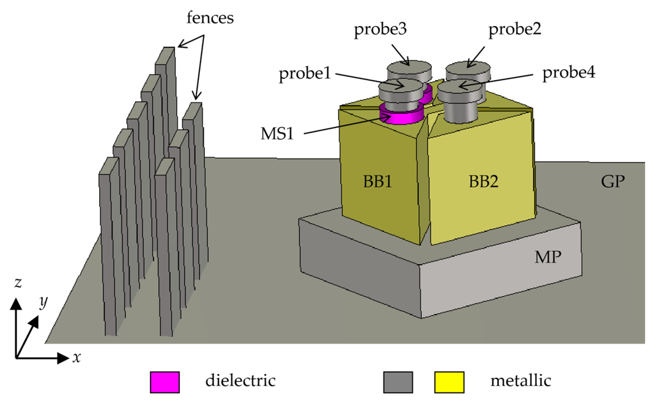
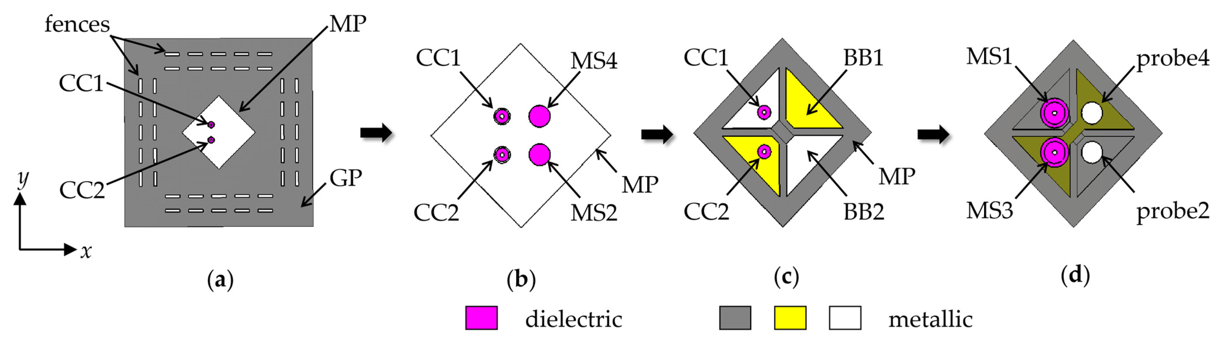
Figure 2 exhibits the details of the evolution of the feed structure through the cutting plane view. The whole antenna has two coaxial cables, so-called CC1 and CC2, to feed four dipole vibrators. Figure 2a,b present the evolution of CC1. The inner conductor IC1 is directly soldered to probe1. The outer conductor OC1 transforms into the bow-tie balun BB1 and probe2. Probe1 and probe2 are separately soldered to vibrator1 and vibrator2. These two vibrators are hidden in Figure 2. Throughout this process, bridge1 at the top of BB1 realizes the connection between OC1 and vibrator2. Summarily, IC1 feeds vibrator1, and OC1 feeds vibrator2. Probe1 and probe2 achieve wider-band impedance matching between the coaxial cable and dipole antenna. The second coaxial cable, CC2, experiences the same evolution, as shown in Figure 2d–f. The only difference is that bridge2 of the bow-tie balun BB2 is located at the bottom of BB2. Both BB1 and BB2 have cylindrical hollow openings CO1 and CO2 for the vertical insertion of two mechanical support MS2 and MS4, which are shown later.
If CC1 feeds the antenna to realize vertically polarized (VP) EM radiation, then CC2 realizes orthogonal horizontally polarized (HP) radiation. So, based on the two orthogonal polarizations, the whole antenna structure can be divided into two parts: the vertical polarization part (VPP) and the horizontal polarization part (HPP).
For clarity, Figure 3 shows the 2-D schematic of VPP, including the antenna vibrators, the feed structure, and the ground reflector. The working mechanism and installation of HPP are the same as those of VPP.
In Figure 3, the inner conductor IC1 of the coaxial cable CC1, the metallic probe probe1, and the dipole antenna arm vibrator1 are all connected together and have the same electric potential. The outer conductor OC1 of CC1, the metallic balun BB1, the probe probe2, and vibrator2 are all soldered together to form the opposite electric potential. Two functional dielectric blocks with a relative permittivity of should be introduced here. To prevent probe1 from being shorted by BB1, MS1 provides mechanical and non-conducting support for probe1. MS2 provides the mechanical support for BB1. In addition to this mechanical support, MS2 creates a slot between BB1 and MP. This slot works as a choke to prevent the common mode current from flowing back to the ground plate GP. The red “x” shown in Figure 3 means the common mode current is unwanted.
Furthermore, two rows of metallic fences are vertically installed on each edge of GP to prevent lateral wave leakage. If only one row of fences on each side is installed, it cannot effectively prevent the wave leakage. If three rows or more rows than two rows are chosen, the complexion and weight of the structure are abruptly increased.
Figure 4 shows the 3-D view of the proposed feed structure and ground reflector. The vibrator layer, parts of fences, and GP are hidden for a better view. The dielectric blocks are in magenta. To highlight the proposed metallic bow-tie baluns (BBs), they are shown in yellow, different from other metallic structures in gray, such as MP, GP, fences, etc.
2.2. Bow-Tie Balun
Figure 5 shows the explosion view of the feed structure for VPP.
During the manufacturing process, the hat-shaped probes, probe2, and BB1 are fabricated together as one metallic block. BB1 has two wings, wing1, and wing2. These wings are transformed from the outer conductor, OC1. In the implement, wing1 has a through hole TH1. CC1 can go through BB1 from the bottom to the top through this hole. BB1 has a larger surface area than OC1. So, the resonant common mode current is disturbed by this bow-tie-shaped balun. Meanwhile, the slot mentioned in Section 2.1 chokes from going back to the ground plate GP. Compared with the conventional coaxial cable, the combination of the hat-shaped probes, the bow-tie shaped balun, and the slot between the balun and the ground achieves a wider impedance match. Figure 6 presents the installation of the two bow-tie baluns, BB1 and BB2. BB1 is orthogonally inserted into BB2. BB2 has a through hole in TH2 as well. Both BB1 and BB2 are firmly supported by the mechanical supports MS2 and MS4.
2.3. Antenna Vibrator
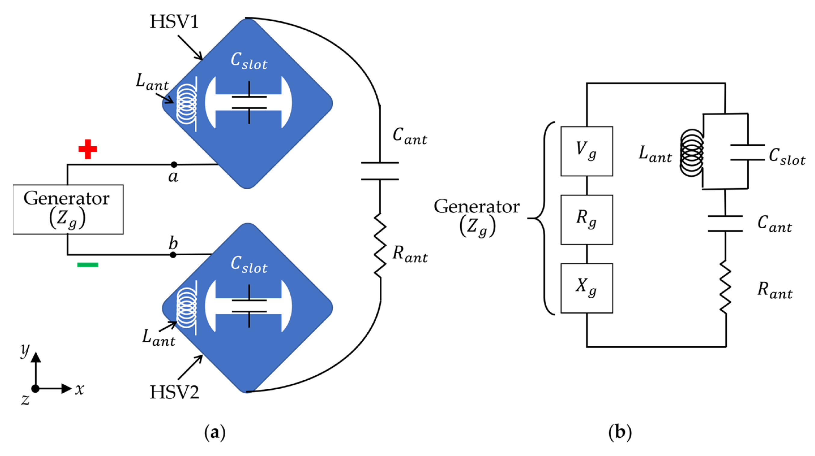
Four antenna vibrators are etched on the top layer of a dielectric substrate with a dielectric constant of 2.2 and a loss tangent of 0.0009, which is the same as the dielectric substrate of MS1~MS4. The dielectric substrate has four through holes. The four probes underneath go through these holes and are separately soldered to the four square vibrators. Figure 7a shows the regular dipole antenna with two square vibrators, SV1 and SV2, in transmitting mode [40] (pp. 75–79). This pair of vibrators produces one polarized radiation. Transmission line a connects the generator and SV1. Transmission line b connects the generator and SV2. Figure 7b illustrates the equivalent circuit model (ECM) of this antenna. is the inductive value of SV1 and SV2. is the capacitive value between SV1 and SV2. equals the radiation resistor of the antenna. When the series resonance occurs between and , the maximum EM energy is radiated. When the frequency is lower than the resonant frequency , this series circuit has a capacitive reactance. When the frequency is higher than , it has an inductive reactance.
In Figure 8a, each square vibrator of the dipole antenna is loaded with an H-shaped slot and is named HSV1 or HSV2. This dipole antenna is in transmitting mode as well. This H-shaped slot works as a capacitor . A parallel resonant circuit is composed of and , as shown in Figure 8b. When the frequency is low, this parallel circuit works as an inductor . So, the whole circuit is similar to the one in Figure 7b. When the frequency is high, this parallel circuit works as a capacitor . So, the circuit has a capacitive reactance . Obviously, this capacitive slot enhances the EM radiation, especially in the higher frequency band. This point is verified in the next section.
3. Parametric Study and Design Guidelines
3.1. The Dimensional Parameters
For a better understanding of the whole antenna, several cutting planes are shown first. Then its dimensional parameters are presented. The key dimensional parameters are studied in detail. Finally, the design guidelines for this antenna are expanded.
Figure 9 shows the side view of the cutting plane along the xoz plane. It has four red dashed lines, such as a-a’, b-b’, c-c’, and d-d’, to indicate the locations of the cutting planes along the xoy plane shown in Figure 10. The dielectric area is shown in magenta and the metallic area is in yellow and white in Figure 9. Only BB1 is shown in yellow.
Figure 10 exhibits the four cutting planes along the xoy plane, including a-a’, b-b’, c-c’ and d-d’, along the xoy plane. These are the top views of the whole structure shown. In each figure of Figure 10, the metallic area in dark gray represents the area beneath the cutting plane. The metallic area in white or yellow belongs to the current cutting plane. To achieve an easier understanding, BB1 and BB2 are separately shown in different colors: yellow and white.
Figure 11 illustrates the dimensional parameters according to the cutting plane along the xoz plane. The dimensional parameters of the probes, the mechanic supports, the bow-tie baluns, the slot, the metallic plate, the ground plate, and the fences are included.
The dimensional parameters shown in Figure 11 are listed in Table 1. These values are achieved through investigation and optimization.
Figure 12 exhibits the rest dimensional parameters on three cutting planes along the xoy plane. Figure 12a,b show the border lines of the antenna dielectric substrate. Four antenna vibrators are etched on the top layer of this dielectric substrate. Four through-holes, or vias in short, are drilled near the center of the substrate, as shown in Figure 12a. The four probes can go through the vias and be directly soldered to the four vibrators. In Figure 12b, the bow-tie baluns BB1 and BB2 are zoomed in to reveal the details of the dimensional parameters. Figure 12c mainly reveals the dimensional parameters of the fences. The side lengths of the antenna dielectric substrate and the ground plate GP are the same.
3.2. The Parametric Study
3.2.1. The Isolation of the Ports of the Bow-Tie Baluns
Since the structural parameters of the proposed bow-tie baluns are important and sensitive for impedance matching and operating bandwidth, the parametric study mainly focuses on them. Firstly, there are two input ports, port1 of CC1 and port2 of CC2. Port1 is an excited port. port3 and port4 are two discrete output ports. Port3 is between probe1 and probe2. port 4 is between probe3 and probe4. As shown in Figure 13a, the antenna vibrators and the fences are not contained, and GP is hidden for a better view in this model.
When port1 is excited, the antenna vibrators connecting to port3 realize one polariztions. When port2 is excited, the orthogonal polarization is obtained by two vibrators attached to port4. The isolation between port1 and port2 and the one between port1 and port4 are both roughly higher than 20 dB within the whole working band. When the vibrators are connected to the probes, the reflection and transmission coefficients of the input ports, such as and , can be improved further.
Then, the antenna vibrators and fences are included in the model as a whole structure. The height hBB, width lBB3 and gap gBB between the baluns are investigated. The simulated results are presented below. Finally, the slot between the bow-tie balun and the MP is explored.
3.2.2. The Height of the Bow-Tie Balun hBB
The height of the bow-tie balun hBB is an important parameter. First of all, it directly determines the distance between the antenna vibrators and the ground plate. Commonly, this distance equals a quarter wavelength of the central frequency point within the operating frequency band. So, if hBB is quite small, the crossed dipole antenna cannot obtain good radiation characteristics, especially in the low frequency band. Secondly, if hBB is large, it means that the feed lines are too long and may cause higher harmonics and impedance mismatching. As shown in Figure 14, when hBB = 15 mm or hBB = 20 mm, the reflection coefficient S11 of the feed port rises to more than −10 dB around 5 GHz. Thirdly, if hBB is large, the whole structure cannot be defined as a low-profile antenna.
3.2.3. The Side Length of the Bow-Tie Balun lBB3
The relation between the side length of the bow-tie balun lBB3 and S11 is studied. The simulated results are presented in Figure 15. When lBB3 = 11 mm, it means that the bow-tie baluns are very compact. It is not easy for installation, such as letting the coaxial cables go through them and being fixed on top of MP. When lBB3 increases from 11 mm, the impedance matching around 5 GHz is improved. The reflection coefficient S11 is lower than −10 dB from 2.5 GHz to 6.5 GHz when lBB3 is from 12 mm to 15 mm. When lBB3 > 15 mm, the impedance mismatch within the band occurs again.
3.2.4. The Gap between Two Bow-Tie Baluns gBB
The gap between two bow-tie baluns gBB is a key dimensional parameter for the impedance matching. Figure 16 shows the relation between this gap gBB and S11. If gBB is smaller than 1 mm, the antenna vibrators are prone to attaching to each other, which cannot generate differential signals between vibrators. Obviously, as the value of gBB increases, the bridges bridge1 and bridge2 are elongated, and the operating bandwidth becomes narrower. When gBB = 4 mm, the operating bandwidth is half that of the one with gBB = 1 mm. The reason is that when the length of the bridges increases, the phase difference between the two currents and increases as well. This phase difference worsens the wideband impedance matching.
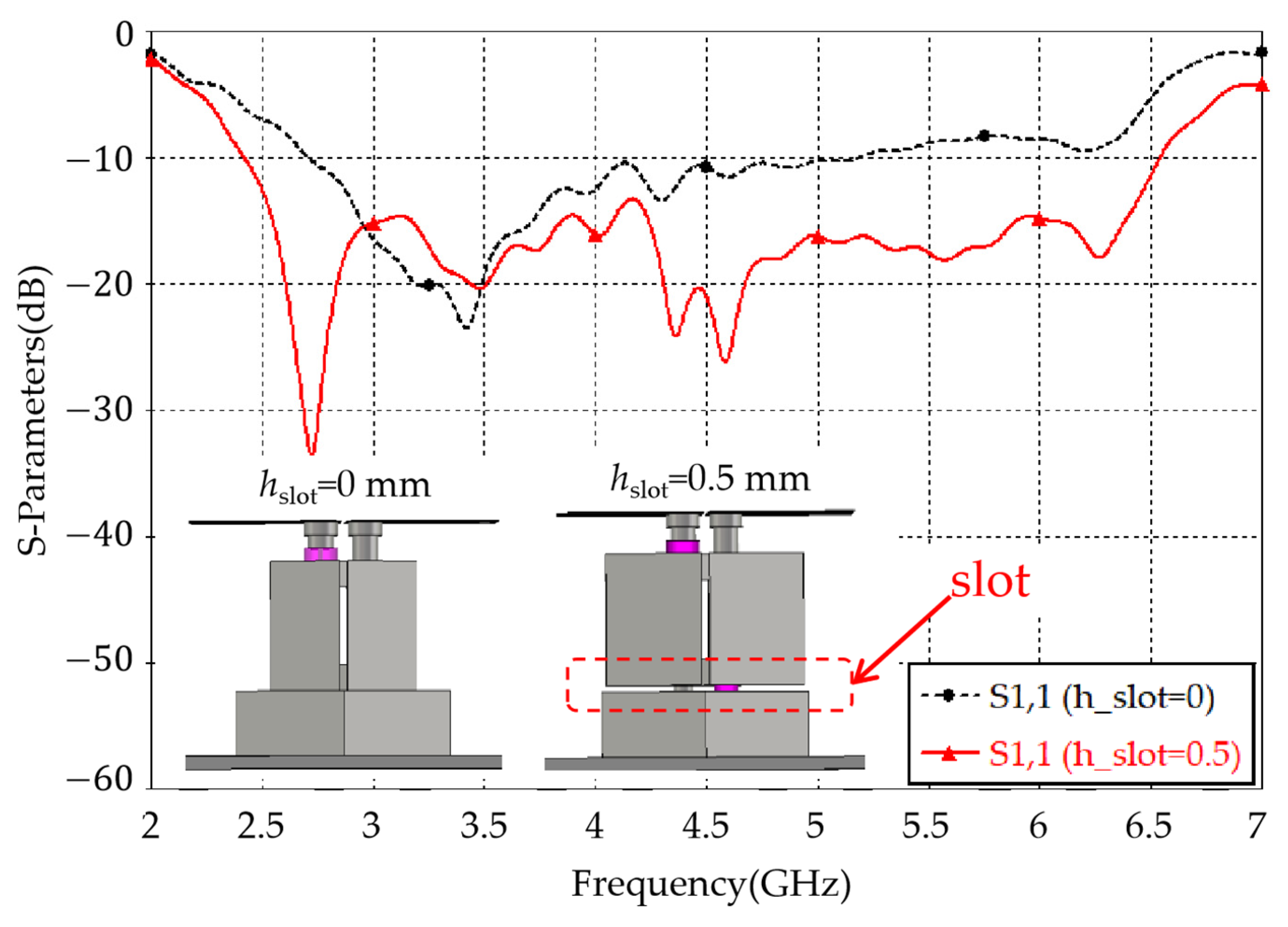
3.2.5. The Height of the Slot between Two Bow-Tie Baluns and MP hslot
To lower the profile of this proposed antenna, the height of the slot is expected to be as small as possible. For this reason, as shown in Figure 17, only two situations are investigated. The first situation (hslot = 0 mm) means that the structure has no slot between the bow-tie baluns and MP. The second situation (hslot = 0.5 mm) means that a slot works as a choke coil to suppress the common mode current . Through this method, the operating band is nearly doubled.
3.3. Design Guideline
To design this antenna, the central frequency and the wavelength of the operating frequency band are first calculated. Based on the wavelength , the dimensions of each antenna dipole vibrator and the distance between the vibrators and the ground plate are roughly obtained. Both of them are nearly a quarter wavelength . Then, the initial dimensional parameters of the bow-tie balun can be reasonably chosen and optimized according to the parametric study above. Furthermore, the dimensions of MP, GP, and fences are optimized. The number of fences can be optimized to prevent wave leakage. During the whole design procedure, the installation convenience and the limited space between the dipole antenna and the ground plate should be considered.
4. Simulated and Experimental Results
4.1. The Simulated Radiation Characteristics of the Dipole Antennas
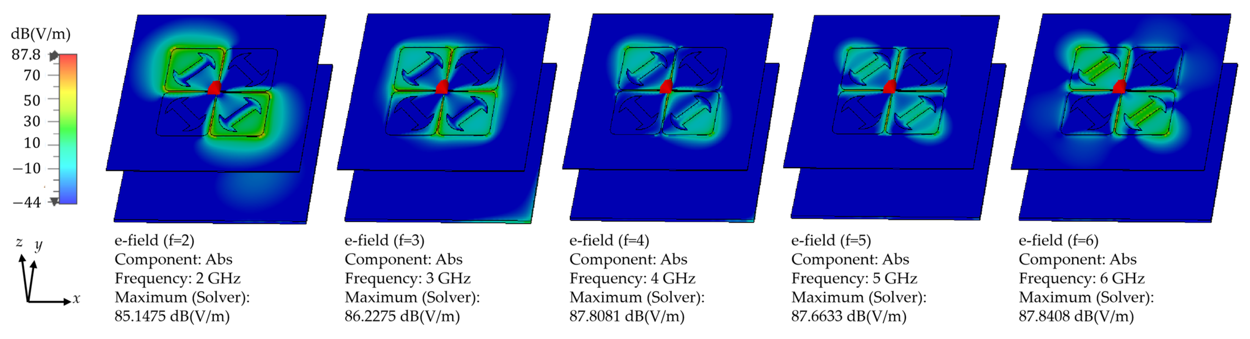
The dipole antennas with SVs and with HSVs, separately shown in Figure 7 and Figure 8, are modeled, simulated, and compared. Only the four vibrators, the dielectric substrate, the metallic ground plate GP, and one discrete port with 50 Ω impedance are included in these models. Figure 18 presents the simulated absolute values of the electric field of the dipole antenna with SVs at different frequency points. Since the tangent electric field on the ideal metallic surface equals zero, the main contribution to the absolute values of the electric field is from the normal electric field . Obviously, the electric field concentrates primarily on the edges of the metallic area. As the frequency increases, the resonant area of the vibrators decreases. Meanwhile, in the central area of each square vibrator, the EM energy becomes less and less. There is some EM coupling between the excited vibrators and the neighboring unexcited ones. As shown in Figure 18, the variation of the electric field values is roughly within 3 dB.
Figure 19 exhibits the simulated 3-D radiation patterns of the dipole antenna with SVs at different frequency points. Since GP is under the antenna substrate, the EM energy radiates along the z axis. The variation of the simulated realized gain of this antenna is around 3 dBi.
Figure 20 explores the simulated absolute values of the electric field of the dipole antenna with HSVs at different frequency points. It can be concluded that at a lower frequency band, such as from 2 GHz to 3 GHz, the electric field mostly locates at the edges of each vibrator, and at a higher frequency band, such as from 4 to 6 GHz, the electric field largely occupies the H-shaped slots. As shown in Figure 20, the variation of the electric field values is nearly within 2 dB.
Figure 21 expands the simulated 3-D radiation patterns of the dipole antenna with HSVs at different frequency points. Within the operating band, the main beam of this antenna is in the z direction. The variation of the realized gain within the band is less than 2 dB. The H-shaped slots help the antenna concentrate the EM energy on the vibrators while maintaining stable radiation characteristics within a wider operating band.
Obviously, the radiation characteristics of the dipole antenna with HSVs are much better than those of the dipole antenna with SVs.
4.2. The Effect of the Fences
4.2.1. The EM Characteristic Comparison of the Models with and without the Fences
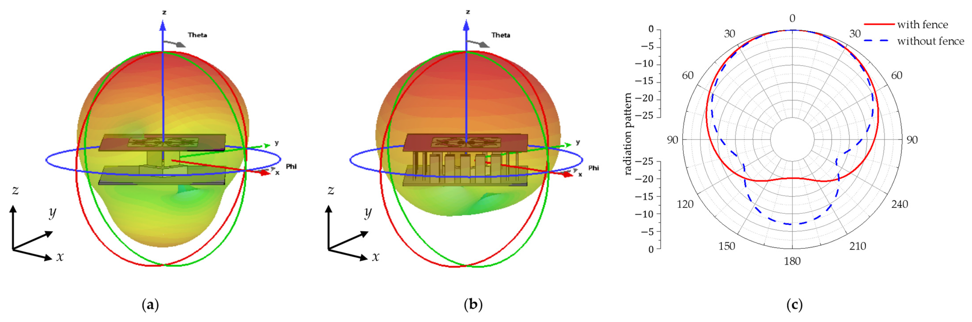
The EM energy radiated by the antenna vibrators travels in both z and z directions. The fences work together with GP as a reflector. So, when the EM wave traveling along the z direction meets the reflector, it will be reflected back to travel along the z direction. The fences help the antenna concentrate the radiated EM energy in the z direction, especially in the lower frequency band. Figure 22 shows the comparison of the 3D and 2D radiation patterns of the models with and without the fences at 2 GHz.
As obviously seen in Figure 22, the fences do effectively prevent the EM energy from leaking in the back direction, which is the z direction.
4.2.2. The Effect of the Fences at Different Frequencies
The effect of the fences at different frequencies is investigated by observing the surface current of the whole structure at different frequencies, as shown in Figure 23. Firstly, the variation of the maximum surface current values from 3 GHz to 6 GHz is within 1 dB(A/m). It verifies the stability of its EM characteristics. Secondly, as shown in these figures, the inner row of fences located on each side of the ground plate has a stronger induced current than the outer row, which verifies the effect of the fences, and two rows are needed and better. At 4 GHz, a stronger resonance than the ones at other frequencies occurs on the surfaces of the fences. This resonance is the reason for a higher reflection coefficient around 4 GHz.
4.3. The Experimental Results
The bow-tie balun-fed dual-polarized crossed dipole antenna is fabricated and measured. Its photographs are shown in Figure 24.
In Figure 24a, the structures under the antenna dielectric substrate are exhibited from a top view. There are two rows of fences soldered on the upper side of GP and another two rows on its left side. On the right and lower sides, four rows of fence slots (FSs) are presented. These FSs are for the vertical installation of fences. After each fence is vertically inserted into one FS, the fence is soldered to the GP. MP, two bow-tie baluns (BB1 and BB2), four probes (probe1~probe4) are shown out. Especially, the inner conductors (IC1 and IC2) go through the probes (probe1 and probe3) from the bottom, as clearly shown in Figure 24a. GP and MP are mechanically fabricated as one metallic block. Soldering between them is not needed. Figure 24b illustrates the side view of the structure without the antenna layer and some fences. MS1 and slot can be easily viewed in this photograph. MS1 shown in Figure 24b and MS3 shown in Figure 10 guarantee the installation of probe1 and probe3. MS2 and MS4, which are shown in Figure 10, provide the alignment of the bow-tie baluns on MP and offer the slot between the bow-tie baluns and MP. The metallic part of the whole structure is made of copper, which can be easily soldered. The fabrication tolerance is within 0.2 mm. To achieve better port isolation, two 50 Ω/sq resistive films etched on a dielectric substrate with a dielectric constant of 2.2 and a thickness of 0.5 mm are inserted in the gaps between the two bow-tie baluns. Figure 24c shows the setup for the reflection coefficient measurement. A vector network analyzer (VNA) is utilized to do the test. In the antenna aperture, four HSVs are clearly exhibited. The EM characteristics of the proposed antenna ports are measured. The simulated and measured results of S11 representing the reflection coefficient, and S21 indicating the port isolation, are presented in Figure 25.
As seen in Figure 25, the measured operating frequency band for is from 2.42 GHz to 6.48 GHz. The fractional bandwidth is 91.2%. Owing to the contributions of the two resistive films between the two baluns, the measured port isolation is improved and lower than −20 dB within the band.
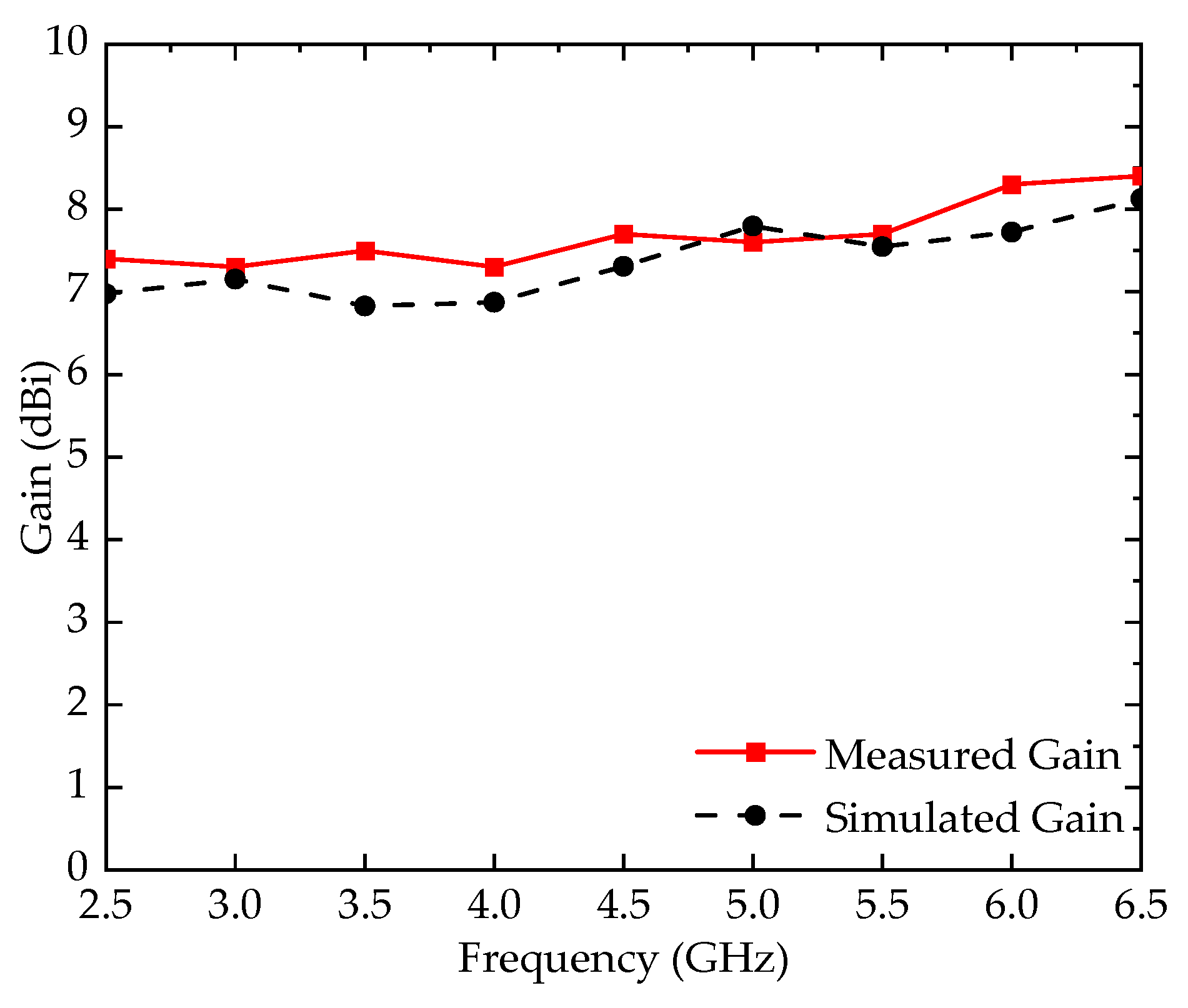
Figure 26 shows the setup for the radiation characteristics measurement in an anechoic chamber. The gain and radiation patterns are measured.
The realized gain of the proposed dipole antenna with HSVs is measured. A standard wideband horn antenna is needed for the measurement. Firstly, the electric level of this horn antenna in the main beam direction is measured in the anechoic chamber. Then, the same measurement is done for the proposed antenna. The electric level difference between these two measurements is obtained. The gain of the standard horn antenna can be found on its data sheet. So, the gain of the proposed antenna equals the gain of the standard horn antenna plus the measured electric level difference. Finally, The measured gain of the proposed antenna within the operating band is presented in Figure 27. The proposed antenna achieves a realized gain of within the band. The realized gain is the value at the fixed boresight direction. Compared with the discrete port with 50 Ω impedance, the tapering probes realize wider band impedance matching and wider band electromagnetic radiation stability.
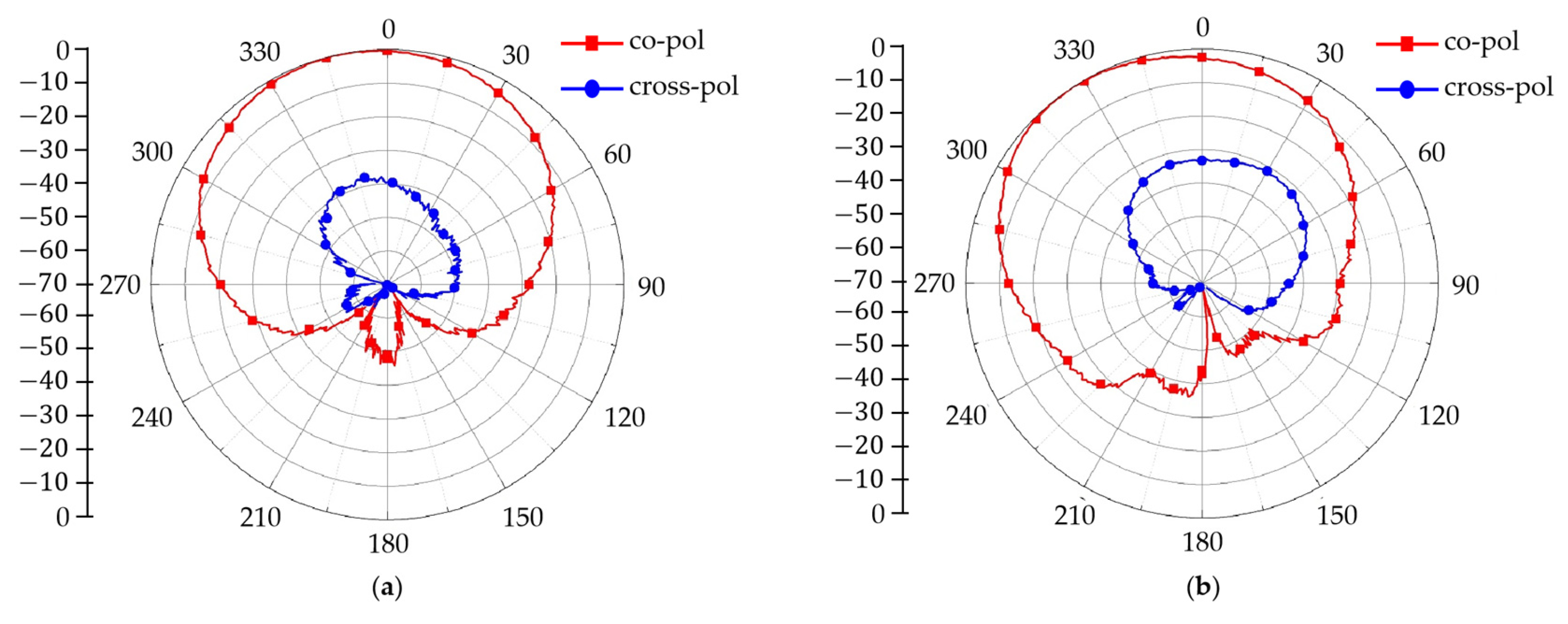
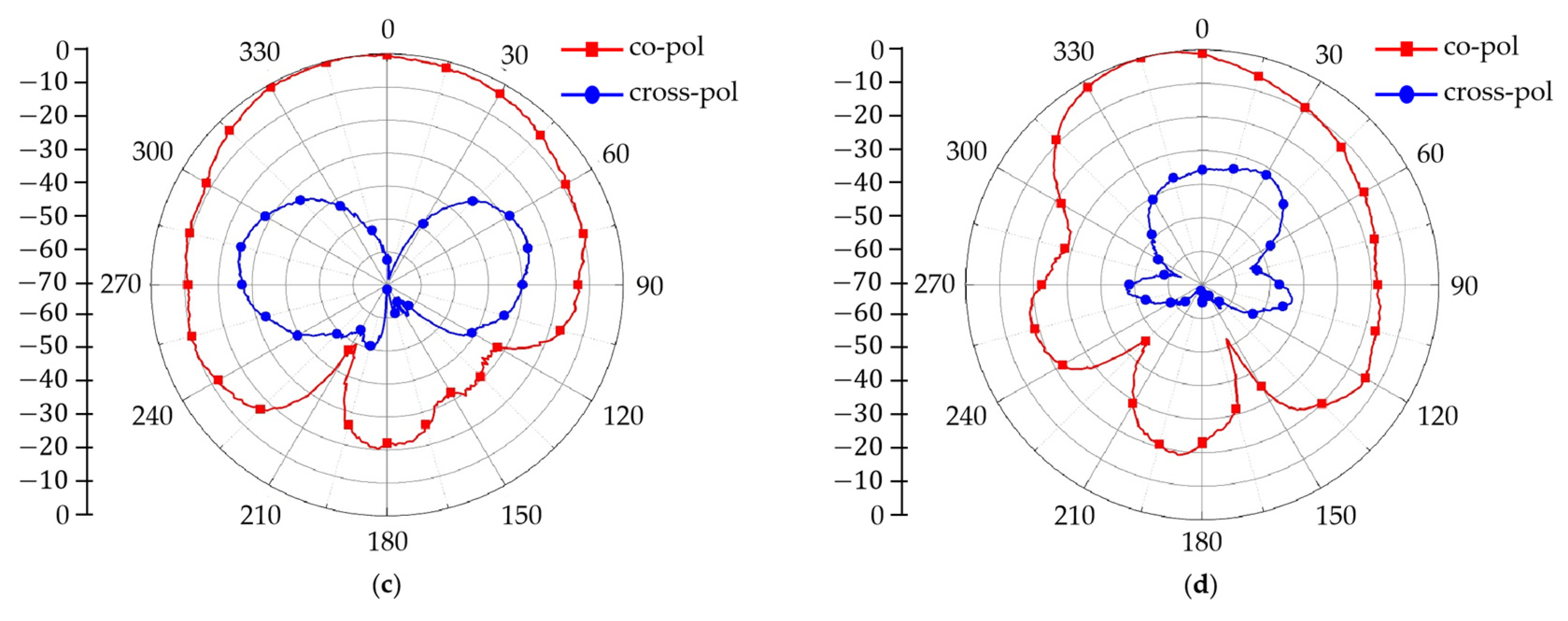
The measured E-plane radiation patterns at different frequencies are exhibited in Figure 28, and the measured H-plane ones are shown in Figure 29. Since the bridge between two wings of each bow-tie balun generates an extra minor phase difference between and it is the reason behind the beam tilting towards at some higher frequencies in Figure 28.
In these two figures, the radiation patterns within the operating band from 2.42 to 6.48 GHz are expanded. The cross-polarization discrimination ratio (XPD) is better than 25 dB within the band. When the frequency is low, it has weaker directivity. When the frequency increases, the directivity of the E-plane pattern occurs. The stability of the H-plane patterns is better than that of the E-plane patterns.
Table 3 is the comparison table of the related state-of-the-art dual-polarized crossed dipole antennas and the proposed one in this paper.
Compared with these references, in the case in which a low profile and compact size are achieved, the proposed antenna has a higher XPD; in the other case, in which roughly the same gain is obtained within the band, the proposed antenna has a wider bandwidth or a higher port isolation.
5. Conclusions
In this paper, a broadband dual-polarized crossed dipole antenna is proposed. First of all, the operational principle, the bow-tie balun, and the antenna vibrator are introduced. Then, the key dimensional parameters are investigated. According to these studies, the design guidelines for this proposed antenna were derived. Finally, this proposed antenna is fabricated and measured. The simulated and measured results show that the antenna has a wide impedance bandwidth from 2.42 GHz to 6.48 GHz. The fractional bandwidth is 91.2%. Moreover, within the whole band, the E-plane and H-plane radiation patterns are stable. The port isolation is greater than 20 dB, and the cross-polarization discrimination ratio is better than 25 dB. The proposed antenna achieves a realized gain of . It can be a good candidate for sub-6 GHz wireless communications or short-range radar applications.
Author Contributions
Software, T.S.; Validation, X.H.; Data curation, Y.X.; Writing—original draft, W.W.; Project administration, N.Y. All authors have read and agreed to the published version of the manuscript.
Funding
This research was funded by National Defense Science and Technology Innovation Fund of the Chinese Academy, grant number 2022-JCJQ-JJ-0230.
Data Availability Statement
The data that support the findings of this study are available from the corresponding author, W.W., upon reasonable request.
Conflicts of Interest
The authors declare no conflict of interest.
References
- Wang, B.; Liao, C.; Du, C.H. A Low-Profile Broadband Dual-Polarized Base Station Antenna Array With Well-Suppressed Cross-Polarization. IEEE Trans. Antennas Propag. 2021, 69, 8354–8365. [Google Scholar] [CrossRef]
- Li, Y.; Chu, Q.X. Shared-Radiator Design of Dual-Band Coplanar Base Station Antenna Array Using Cavity-Backed Slots. IEEE Trans. Antennas Propag. 2021, 69, 8985–8990. [Google Scholar] [CrossRef]
- Liu, X.; Gao, S.; Hu, W.; Wen, L.; Luo, Q.; Sanz-Izquierdo, B.; Yang, X.X. A Compact Dual-Polarized Filtering Antenna With Steep Cut-Off for Base-Station Applications. IEEE Trans. Antennas Propag. 2022, 70, 5941–5946. [Google Scholar] [CrossRef]
- He, Y.; Huang, W.; He, Z.; Zhang, L.; Gao, X.; Zeng, Z. A Novel Cross-Band Decoupled Shared-Aperture Base Station Antenna Array Unit for 5G Mobile Communications. IEEE Open J. Antennas Propag. 2022, 3, 583–593. [Google Scholar] [CrossRef]
- Li, J.; Hao, S.J.; Cui, Y.G.; Chen, X. A Miniaturized Wideband Dual-Polarized Planar Antenna Based on Multiresonance. IEEE Antennas Wirel. Propag. Lett. 2022, 21, 242–246. [Google Scholar] [CrossRef]
- Ye, L.H.; Yuanjun, L.; Wu, D.L. Dual-Wideband Dual-Polarized Dipole Antenna With T-Shaped Slots and Stable Radiation Pattern. IEEE Antennas Wirel. Propag. Lett. 2022, 21, 610–614. [Google Scholar] [CrossRef]
- Han, B.; Wu, Q.; Yu, C.; Wang, H.; Gao, X.; Ma, N. Ultracompact Dual-Polarized Cross-Dipole Antenna for a 5G Base Station Array With a Low Wind Load. IEEE Trans. Antennas Propag. 2022, 70, 9315–9325. [Google Scholar] [CrossRef]
- Xiong, H.Q.; Zhang, C.J.; Tong, M.S. Wideband Low-Profile Dual-Polarized Antenna Based on a Gain-Enhanced EBG Reflector. IEEE Trans. Compon. Packag. Manuf. Technol. 2022, 12, 391–394. [Google Scholar] [CrossRef]
- Biswas, S. Wideband and Dual-Polarized Crossed Dipole Antenna Design Using Substrate-Integrated Coax. IEEE Open J. Antennas Propag. 2023, 4, 361–372. [Google Scholar] [CrossRef]
- Qin, Y.; Zhang, L.; Mao, C.X.; Zhu, H. A Compact Wideband Antenna With Suppressed Mutual Coupling for 5G MIMO Applications. IEEE Antennas Wirel. Propag. Lett. 2023, 22, 938–942. [Google Scholar] [CrossRef]
- Jiang, J.; Chu, Q.X. Dual-Band Shared-Aperture Base Station Antenna Array Based on 3-D Chokes. IEEE Antennas Wirel. Propag. Lett. 2023, 22, 824–828. [Google Scholar] [CrossRef]
- Peng, J.D.; Li, X.L.; Ye, L.H.; Li, J.F.; Wu, D.L.; Zhang, X.Y. Low-Profile Wideband Dual-Polarized Dipole Antenna With Parasitic Strips and Posts. IEEE Antennas Wirel. Propag. Lett. 2023, 22, 844–848. [Google Scholar] [CrossRef]
- Ye, L.H.; Chen, Z.; Li, J.F. Ultra-Wideband Dual-Polarized Base-Station Antenna With Stable Radiation Pattern. IEEE Trans. Antennas Propag. 2023, 71, 1919–1924. [Google Scholar] [CrossRef]
- Tan, X.; Mei, X.; Wu, K.L. XPD Enhancement of Dipole Antenna Arrays by Inducing Coherent Current From Feeding Line. IEEE Trans. Antennas Propag. 2023, 71, 3950–3958. [Google Scholar] [CrossRef]
- Fu, S.; Cao, Z.; Quan, X.; Xu, C. A Broadband Dual-Polarized Notched-Band Antenna for 2/3/4/5G Base Station. IEEE Antennas Wirel. Propag. Lett. 2020, 19, 69–73. [Google Scholar] [CrossRef]
- Ou, J.H.; Chen, Z.; Bo, S.F.; Zhang, Y.; Zhang, X.Y. Compact Dual-Polarized Antenna with Low-Pass Response for Marine Communication. IEEE Trans. Veh. Technol. 2021, 70, 2649–2656. [Google Scholar] [CrossRef]
- Liu, X.; Gao, S.; Sanz-Izquierdo, B.; Zhang, H.; Wen, L.; Hu, W.; Yang, X.X. A Mutual-Coupling-Suppressed Dual-Band Dual-Polarized Base Station Antenna Using Multiple Folded-Dipole Antenna. IEEE Trans. Antennas Propag. 2022, 70, 11582–11594. [Google Scholar] [CrossRef]
- Yang, S.J.; Duan, W.; Liu, Y.Y.; Ye, H.; Yang, H.; Zhang, X.Y. Compact Dual-Band Base-Station Antenna Using Filtering Elements. IEEE Trans. Antennas Propag. 2022, 70, 7106–7111. [Google Scholar] [CrossRef]
- Yang, W.; Li, Y.; Xue, Q.; Liao, S.; Che, W. Miniaturized Broadband Dual-Polarized Dipole Antenna Based on Multiple Resonances and its Array for Base-Station Applications. IEEE Trans. Antennas Propag. 2022, 70, 11188–11193. [Google Scholar] [CrossRef]
- Yang, S.J.; Ma, R.; Zhang, X.Y. Self-Decoupled Dual-Band Dual-Polarized Aperture-Shared Antenna Array. IEEE Trans. Antennas Propag. 2022, 70, 4890–4895. [Google Scholar] [CrossRef]
- Li, Y.; Chu, Q.X. Dual-Band Base Station Antenna Array Using the Low-Band Antenna as Parasitic Decoupler. IEEE Antennas Wirel. Propag. Lett. 2022, 21, 1308–1312. [Google Scholar] [CrossRef]
- Chen, Z.; Xu, T.; Li, J.F.; Ye, L.H.; Wu, D.L. Dual-Broadband Dual-Polarized Base Station Antenna Array With Stable Radiation Pattern. IEEE Antennas Wirel. Propag. Lett. 2023, 22, 303–307. [Google Scholar] [CrossRef]
- Liu, Y.; Yue, Z.; Jia, Y.; Xu, Y.; Xue, Q. Dual-Band Dual-Circularly Polarized Antenna Array With Printed Ridge Gap Waveguide. IEEE Trans. Antennas Propag. 2021, 69, 5118–5123. [Google Scholar] [CrossRef]
- Yang, D.; Zhai, H.; Guo, C.; Ma, C. A Novel Differentially Fed Dual-Polarized Filtering Magneto-Electric Dipole Antenna for 5G Base Station Applications. IEEE Trans. Antennas Propag. 2022, 70, 5373–5382. [Google Scholar] [CrossRef]
- Liang, M.S.; Zhou, Y.; Yang, X.S.; Wu, P.F. A Low-Profile Dual-Polarized Substrate Integrated Magneto-Electric Dipole MIMO Antenna. IEEE Antennas Wirel. Propag. Lett. 2023, 22, 1431–1435. [Google Scholar] [CrossRef]
- Wu, S.; Shang, F. Broadband Dual-Polarized Magnetoelectric Dipole Antenna With Compact Structure for 5G Base Station. IEEE Access 2023, 11, 20806–20813. [Google Scholar] [CrossRef]
- Liu, T.; Zhu, W.J.; Hu, X.J.; Ye, L.H.; Wu, D.L. Dual-Wideband Dual-Polarized Magnetoelectric Dipole Antenna for Sub-6 GHz Applications. IEEE Antennas Wirel. Propag. Lett. 2023, 22, 1396–1400. [Google Scholar] [CrossRef]
- Wu, F.; Wang, J.; Zhang, Y.; Hong, W.; Luk, K.M. A Broadband Circularly Polarized Reflectarray With Magneto-Electric Dipole Elements. IEEE Trans. Antennas Propag. 2021, 69, 7005–7010. [Google Scholar] [CrossRef]
- Zhu, H.; Liu, G.; Wang, K.; Mou, J.; Zhou, Y.; Xie, S.; Di, Y. Ultrawideband Compact Magnetoelectric Dipole Antenna/Array With Dual-Polarization. IEEE Trans. Antennas Propag. 2023, 71, 4504–4509. [Google Scholar] [CrossRef]
- Alexandre, L.C.; De Souza Filho, A.L.; Sodré, A.C. Indoor Coexistence Analysis Among 5G New Radio, LTE-A and NB-IoT in the 700 MHz Band. IEEE Access 2020, 8, 135000–135010. [Google Scholar] [CrossRef]
- El Yousfi, A.; Abdalmalak, K.A.; Lamkaddem, A.; Vargas, D.S. Miniaturized Broadband dual-polarized Dielectric Resonator Antenna Using Characteristic Modes. In Proceedings of the 2023 17th European Conference on Antennas and Propagation (EuCAP), Florence, Italy, 26–31 March 2023; pp. 1–4. [Google Scholar] [CrossRef]
- Abdalmalak, K.A.; Romano, S.L.; García, E.; Lampérez, A.G.; Martínez, F.J.H.; Palma, M.S.; Fernández, J.A.L. Radio astronomy ultra wideband receiver covering the 2–14 GHz frequency band for VGOS applications. In Proceedings of the 2016 10th European Conference on Antennas and Propagation (EuCAP), Davos, Switzerland, 10–15 April 2016; pp. 1–5. [Google Scholar] [CrossRef]
- Dawoud, K.A.A. Analysis and design of antennas and radiometers for radio astronomy applications in microwave, Mm-wave, and THz Bands. Ph.D. Thesis, Universidad Carlos III de Madrid, Madrid, Spain, 2022. Available online: http://hdl.handle.net/10016/35126 (accessed on 1 February 2022).
- Zhang, K.; Tan, R.; Jiang, Z.H.; Huang, Y.; Tang, L.; Hong, W. A Compact, Ultrawideband Dual-Polarized Vivaldi Antenna With Radar Cross Section Reduction. IEEE Antennas Wirel. Propag. Lett. 2022, 21, 1323–1327. [Google Scholar] [CrossRef]
- Lu, J.; Shao, Z.; Li, C.; Gu, C.; Mao, J. A Portable 5.8 GHz Dual Circularly Polarized Interferometric Radar Sensor for Short-Range Motion Sensing. IEEE Trans. Antennas Propag. 2022, 70, 5849–5859. [Google Scholar] [CrossRef]
- Kim, D.; Park, C.Y.; Kim, Y.; Kim, H.; Yoon, Y.J. Four-Arm Sinuous Antenna With Low Input Impedance for Wide Gain Bandwidth. IEEE Access 2022, 10, 35265–35272. [Google Scholar] [CrossRef]
- Sun, H.H.; Cheng, W.; Fan, Z. Diameter Estimation of Cylindrical Metal Bar Using Wideband Dual-Polarized Ground-Penetrating Radar. IEEE Trans. Instrum. Meas. 2023, 72, 8000714. [Google Scholar] [CrossRef]
- Kraus, J.D.; Marhefka, R.J. Antennas for All Applications, 2nd ed.; Publishing House of Electronics Industry: Beijing, China, 2008. [Google Scholar]
- Zheng, Y.; Weng, Z.; Qi, Y.; Fan, J.; Li, F.; Yang, Z.; Drewniak, J.L. Calibration Loop Antenna for Multiple Probe Antenna Measurement System. IEEE Trans. Instrum. Meas. 2020, 69, 5745–5754. [Google Scholar] [CrossRef]
- Balanis, C.A. Antenna Theory Analysis and Design, 3rd ed.; Wiley: Hoboken, NJ, USA, 2016. [Google Scholar]
Figure 1.
A dipole antenna fed by a coaxial cable.

Figure 2.
The evolution of the feed structure: (a) CC1; (b) IC1 loaded with probe1; (c) OC1 loaded with BB1; (d) CC2; (e) IC2 loaded with probe3; (f) OC2 loaded with BB2.
Figure 2.
The evolution of the feed structure: (a) CC1; (b) IC1 loaded with probe1; (c) OC1 loaded with BB1; (d) CC2; (e) IC2 loaded with probe3; (f) OC2 loaded with BB2.

Figure 3.
Schematic of the whole antenna structure for vertical polarization.

Figure 4.
A 3D view of the proposed feed structure and ground reflector.

Figure 5.
Explosion view of the feed structure for VPP.

Figure 6.
The installation of the two bow-tie baluns.

Figure 7.
The regular dipole antenna with two square vibrators and its ECM: (a) The dipole antenna with SVs; (b) the ECM of the dipole antenna with SVs.
Figure 7.
The regular dipole antenna with two square vibrators and its ECM: (a) The dipole antenna with SVs; (b) the ECM of the dipole antenna with SVs.

Figure 8.
The dipole antenna loaded with H-shaped slots and its ECM: (a) The dipole antenna with HSVs; (b) the ECM of the dipole antenna with HSVs.
Figure 8.
The dipole antenna loaded with H-shaped slots and its ECM: (a) The dipole antenna with HSVs; (b) the ECM of the dipole antenna with HSVs.

Figure 9.
The cutting plane along the xoz plane. The red dashed lines (a-a’, b-b’, c-c’, and d-d’) represent the locations of the cutting planes along the xoy plane.
Figure 9.
The cutting plane along the xoz plane. The red dashed lines (a-a’, b-b’, c-c’, and d-d’) represent the locations of the cutting planes along the xoy plane.

Figure 10.
The cutting planes along the xoy plane: (a) a-a’; (b) b-b’; (c) c-c’; (d) d-d’.

Figure 11.
The dimensional parameters according to the cutting plane along the xoz plane.

Figure 12.
The dimensional parameters according to the cutting planes along the xoy plane: (a) The dimensional parameters of the antenna layer; (b) The dimensional parameters of the bow-tie balun; (c) The dimensional parameters of the ground plate and fences.
Figure 12.
The dimensional parameters according to the cutting planes along the xoy plane: (a) The dimensional parameters of the antenna layer; (b) The dimensional parameters of the bow-tie balun; (c) The dimensional parameters of the ground plate and fences.

Figure 13.
The S parameters of four ports: (a) The simulated model; (b) The simulated results of the S parameters of the four ports.
Figure 13.
The S parameters of four ports: (a) The simulated model; (b) The simulated results of the S parameters of the four ports.

Figure 14.
The relation between hBB and the reflection coefficient S11.

Figure 15.
The relation between lBB3 and the reflection coefficient S11.

Figure 16.
The relation between gBB and the reflection coefficient S11.

Figure 17.
The relation between hslot and the reflection coefficient S11.

Figure 18.
The absolute values of the electric field of the dipole antenna with SVs.

Figure 19.
The 3-D radiation patterns of the electric field of the dipole antenna with SVs.

Figure 20.
The absolute values of the electric field of the dipole antenna with HSVs.

Figure 21.
The 3D radiation patterns of the electric field of the dipole antenna with HSVs.

Figure 22.
The 3D and 2D radiation patterns: (a) the 3D radiation pattern of the antenna model without the fences; (b) the 3D radiation pattern of the antenna model with fences; (c) the 2D radiation patterns of (a,b).
Figure 22.
The 3D and 2D radiation patterns: (a) the 3D radiation pattern of the antenna model without the fences; (b) the 3D radiation pattern of the antenna model with fences; (c) the 2D radiation patterns of (a,b).

Figure 23.
The surface current of the dipole antenna with HSVs.

Figure 24.
Photographs of the dipole antenna with HSVs and the test setup for S11: (a) The top view; (b) the side view; (c) the test setup for S11.
Figure 24.
Photographs of the dipole antenna with HSVs and the test setup for S11: (a) The top view; (b) the side view; (c) the test setup for S11.

Figure 25.
The simulated and measured S11 and S21.

Figure 26.
The setup for the radiation characteristics measurement.

Figure 27.
The simulated and measured gain of the proposed antenna.

Figure 28.
The measured E-plane radiation patterns of the proposed antenna: (a) At 3 GHz; (b) at 4 GHz; (c) at 5 GHz; (d) at 6 GHz.
Figure 28.
The measured E-plane radiation patterns of the proposed antenna: (a) At 3 GHz; (b) at 4 GHz; (c) at 5 GHz; (d) at 6 GHz.


Figure 29.
The measured H-plane radiation patterns of the proposed antenna: (a) At 3 GHz; (b) at 4 GHz; (c) at 5 GHz; (d) at 6 GHz.
Figure 29.
The measured H-plane radiation patterns of the proposed antenna: (a) At 3 GHz; (b) at 4 GHz; (c) at 5 GHz; (d) at 6 GHz.


Table 1.
The values of the dimensional parameters shown in Figure 11 (Unit: mm).
Table 1.
The values of the dimensional parameters shown in Figure 11 (Unit: mm).
| Dimensions | Value | Dimensions | Value |
|---|---|---|---|
| Dp1 | 4 | Dp2 | 3 |
| hMS1 | 1 | hMS2 | 4.5 |
| hprobe | 3 | hbri | 1 |
| hslot | 1 | hBB | 10 |
| hMP | 5 | hGP | 2 |
| hant | 18.5 | hfence | 15 |
| dMS3 | 3 | lbri2 | 1.5 |
Table 2.
The values of the dimensional parameters shown in Figure 12 (Unit: mm).
Table 2.
The values of the dimensional parameters shown in Figure 12 (Unit: mm).
| Dimensions | Value | Dimensions | Value |
|---|---|---|---|
| laslot1 | 10 | laslot2 | 14.8 |
| waslot1 | 3.8 | waslot2 | 3 |
| dprobes | 5.3 | gant | 0.5 |
| lant | 36.5 | lgnd | 65 |
| gBB | 1 | lBB1 | 7 |
| lBB2 | 11.5 | lBB3 | 13 |
| lbri1 | 3 | wbri | 1.5 |
| dxfence | 5 | dyfence | 8 |
| wfence | 5 | tfence | 1 |
Table 3.
Comparison of the related state-of-the-art antennas and the proposed one.
| Ref. | Bandwidth | Gain (dBi) | Iso (dB) | XPD (dB) | ||
|---|---|---|---|---|---|---|
| [1] | 51.5% | 4.23 | 0.09 | >28 | >29 | |
| [5] | 91% | 1.79 | 0.13 | >15 | >20 | |
| [9] | 36% | 12.54 | 0.15 | >20 | >16 | |
| [13] | 100% | 3.40 | 0.21 | >20 | >17 | |
| [19] | 32.73% | 0.83 | 0.19 | >20 | >20 | |
| [26] | 53.2% | 4.17 | 0.18 | >22 | >19 | |
| [29] | 133.3% | 3.00 | 0.55 | >18 | >15 | |
| Pro. | 91.2% | 4.45 | 0.15 | >20 | >25 |
* : the longest operating wavelength. : the central frequency within the operating band.
Disclaimer/Publisher’s Note: The statements, opinions and data contained in all publications are solely those of the individual author(s) and contributor(s) and not of MDPI and/or the editor(s). MDPI and/or the editor(s) disclaim responsibility for any injury to people or property resulting from any ideas, methods, instructions or products referred to in the content. |
© 2023 by the authors. Licensee MDPI, Basel, Switzerland. This article is an open access article distributed under the terms and conditions of the Creative Commons Attribution (CC BY) license (https://creativecommons.org/licenses/by/4.0/).
Share and Cite
MDPI and ACS Style
Wu, W.; Yuan, N.; Hu, X.; Xu, Y.; Shi, T. A Novel Bow-Tie Balun-Fed Dual-Polarized Crossed Dipole Antenna. Electronics 2023, 12, 3032. https://0-doi-org.brum.beds.ac.uk/10.3390/electronics12143032
AMA Style
Wu W, Yuan N, Hu X, Xu Y, Shi T. A Novel Bow-Tie Balun-Fed Dual-Polarized Crossed Dipole Antenna. Electronics. 2023; 12(14):3032. https://0-doi-org.brum.beds.ac.uk/10.3390/electronics12143032
Chicago/Turabian StyleWu, Weiwei, Naichang Yuan, Xueyi Hu, Yixuan Xu, and Tongtong Shi. 2023. "A Novel Bow-Tie Balun-Fed Dual-Polarized Crossed Dipole Antenna" Electronics 12, no. 14: 3032. https://0-doi-org.brum.beds.ac.uk/10.3390/electronics12143032
Note that from the first issue of 2016, this journal uses article numbers instead of page numbers. See further details here.