Article

Influence of Doping Concentration and Thickness of Regions on the Performance of InGaN Single Junction-Based Solar Cells: A Simulation Approach

1
Research Center for Applied Science & Technology, Tribhuvan University, Kathmandu 44600, Nepal
2
School of Semiconductor and Chemical Engineering, Jeonbuk National University, Jeonju 54896, Korea
3
Electrical Department, Gabriel Elektro AS, Lebesby Kommune, 9740 Lebesby, Norway
4
Department of Electrical Engineering, Delhi Technological University, Delhi 110042, India
5
Carbon Composite Energy Nanomaterials Research Center, Woosuk University, Wanju 55338, Korea
6
Woosuk Institute of Smart Convergence Life Care (WSCLC), Woosuk University, Wanju 55338, Korea
*
Authors to whom correspondence should be addressed.
These authors contributed equally to this work.
Submission received: 30 May 2022 / Revised: 20 July 2022 / Accepted: 25 July 2022 / Published: 28 July 2022
(This article belongs to the Special Issue Advances in Electrochemical Energy Storage Systems)

Abstract

:
The impact of doping concentration and thickness of n-InGaN and p-InGaN regions on the power conversion efficiency of single junction-based InGaN solar cells was studied by the Silvaco ATLAS simulation software. The doping concentration 5 × 1019 cm−3 and 1 × 1015 cm−3 were optimized for n-InGaN and p-InGaN regions, respectively. The thickness of 300 nm was optimized for both n-InGaN and p-InGaN regions. The highest efficiency of 22.17% with Jsc = 37.68 mA/cm2, Voc = 0.729 V, and FF = 80.61% was achieved at optimized values of doping concentration and thickness of n-InGaN and p-InGaN regions of InGaN solar cells. The simulation study shows the relevance of the Silvaco ATLAS simulation tool, as well as the optimization of doping concentration and thickness of n- and p-InGaN regions for solar cells, which would make the development of high-performance InGaN solar cells low-cost and efficient.

1. Introduction

The necessity for low-cost, reliable, and sustainable energy is increasing day by day [1,2]. The aim is to determine how best to drive down the cost of using solar cells [3,4,5]. It should be conservative to the environment, as well as economically sustainable to do so. Solar energy is also much safer for humans and the environment since it is a lot easier to generate and transport [6,7,8]. Solar cells using III-nitride semiconductors with indium gallium nitride (InGaN) alloy are extensively studied due to their attractive photovoltaic properties such as high tolerance to radiation, high mobility, and large absorption coefficient, allowing thinner layers of material to absorb most of the solar spectrum [9]. The most important advantage of InGaN alloy might be the direct bandgap energy, which can be adjusted according to the indium composition. Thus, InGaN’s energy bandgap can be tuned from 0.7 eV to 3.42 eV, covering approximately the total solar spectrum [10,11], with absorption coefficients of ~105 cm−1 [12]. The tunability of the InGaN bandgap energy over a wide range provides a good spectral match to sunlight, making it a suitable material for photovoltaic solar cells [13,14,15]. The simulated-based single-junction solar cell has an optimum bandgap energy of 1.39 eV.
Indium gallium nitride (InGaN) alloys offer great potential for high-efficiency photovoltaics, yet theoretical promise has not been experimentally demonstrated [16]. Several major challenges remain, including polarization effects, appropriate thickness of the layer, suitable p-type doping, improved surface passivation, and growth of thick, high-quality InGaN layers [17]. Zhang et al. studied the doping densities and thickness of several layers of In0.65Ga0.35N single-junction solar cells for the identification of their performance and found that 20.28% have front and basic regions with a carrier concentration of 5 × 1017 cm−3 in between the n- and p-layers, with a thickness of 270 nm and 130 nm, respectively [18]. Shen et al. studied the properties of an InxGa1-xN (x = 0.04~0.05) tandem solar cell with an AMPS solar cell simulation tool and presented an efficiency of 24.95% [19]. Bellal et al. described the role of the concentrator in an InGaN dual-junction solar cell using the top cell of InGaN (1.64 eV) and the bottom cell of InGaN (0.94 eV) and exhibited an improvement in the efficiency from 23.87% for a tandem solar cell with a concentration rate (X) of 1 sun to 25.72% for the same solar cell device with 30 suns under AM 1.5 illumination and room temperature [20]. Hussain et al. simulated the maximum efficiency of 29.21% for p-i-n (I is intrinsic, 3–0.5–16 µm thickness) layers with doping concentrations of 1 × 1020 cm−3 and 1 × 1018 cm−3 for the n- and p-region, respectively, and presented values of short-circuit current density (Jsc) of 33.15 mA/cm2, Voc of 1.0 V, and FF of 88.03% [21].
Several simulation tools are available for the characterization of the parameters of the solar cells, such as Silvaco ATLAS, SCAPS, TCAD, Sentaurus, TCAD, AFORS-HET, PC1D, etc. [22,23,24]. Khettou et al. studied an InGaN/GaN Schottky solar cell with AM 1.5 illuminations using Silvaco ATLAS and found the efficiency improved from 2.25% to 18.48% and achieved the optimized composition (xIn) of 54%, work function (wf) of 6.3 eV, doping concentration (Nd) of 2 × 1017 cm−3, and InGaN layer thickness of 0.18 μm [25].
In this work, we used the Silvaco ATLAS simulation software to study the performance of InGaN single-junction solar cells by varying doping concentrations and thicknesses of n- and p-regions. Furthermore, we analyzed the short-circuit current density, open-circuit voltage, fill factor, and conversion efficiency of a single junction-based InGaN solar cell. In addition, indium tin oxide (ITO) was used as an ARC layer with a thickness of 100 nm determined at a wavelength of 700 nm [26]. The highest values of Jsc of 37.68 mA/cm2, Voc of 0.729 V, FF of 80.61%, and efficiency of 22.17% were achieved at optimized parameters of doping concentration and thickness of the n- and p-regions of the InGaN solar cell.

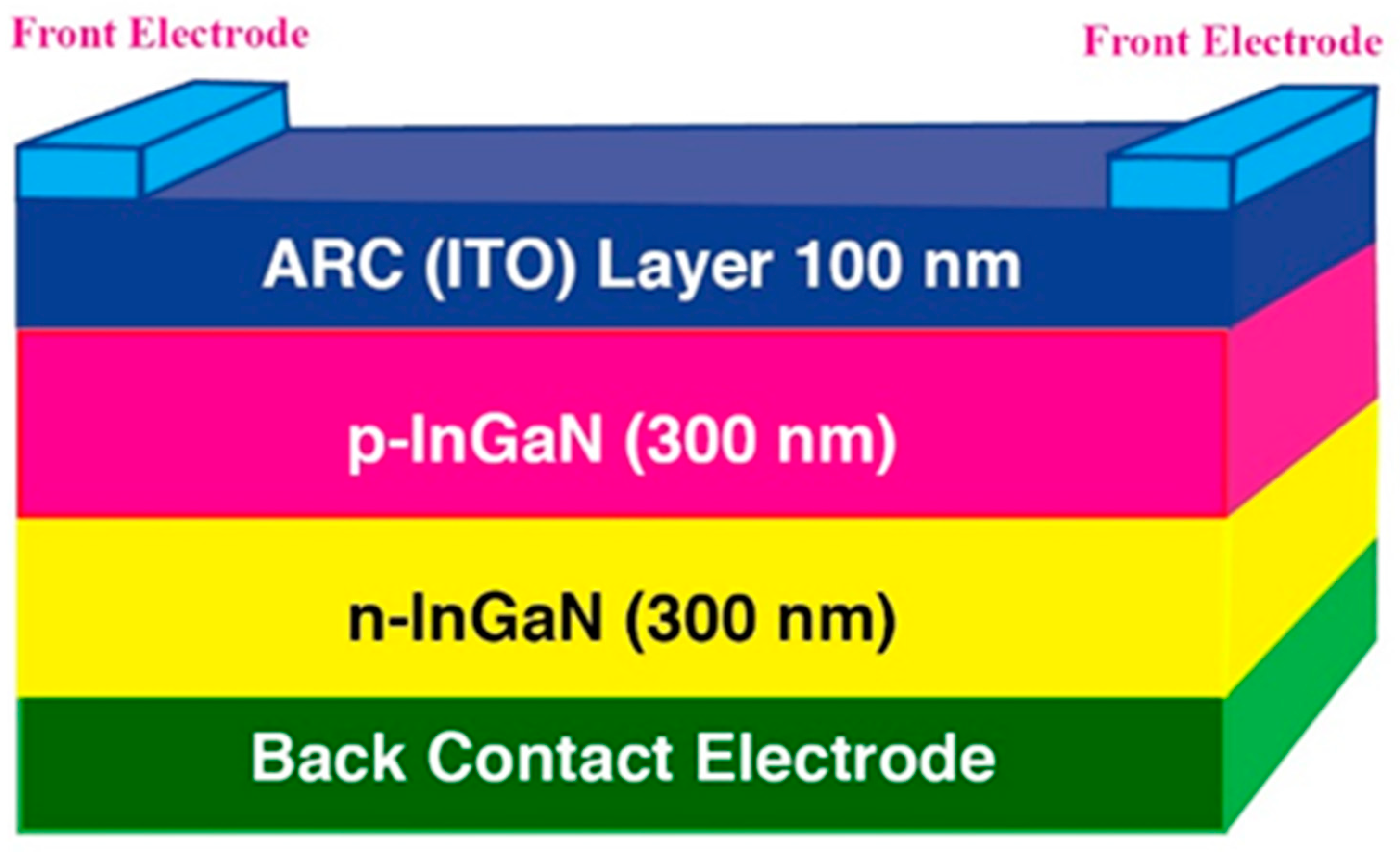
2. Materials and Methods

The schematic device structure of the InGaN single-junction solar cell for investigation is shown in Figure 1. The solar cell configuration consisted of Al/ITO/p-InGaN/n-InGaN/Ag layers where ITO is used as an anti-reflection coating (ARC) layer, aluminum (Al) is a front electrode, and silver (Ag) is in the back contact electrode of the InGaN solar cell. Silvaco ATLAS is a software package used to simulate semiconductor devices. Silvaco software is a simulation that predicts the optical and electrical characteristics related to physical structures and bias conditions.
The operation of a device depends on two- or three-dimensional grid points called nodes [27]. In this work, we made a simulation using Silvaco ATLAS TCAD in 2D. All the parameters of the proposed solar cell in the device structure were carefully selected from the reported works of literature [28,29,30]. Different restrictions were imposed in the calculations, such as incident beam AM1.5G being perpendicular with a certain distance, the propagation of light through every material being identified with the refractive index file, and the surface recombination velocity being taken as 105 m/s for the electron and hole in the interface between the p-InGaN and n-InGaN layer. Simulation software can simulate model semiconductor devices but cannot capture crystalline damage in duckbuild. The calibrated material parameters of the InGaN structure are listed in Table 1.

3. Results and Discussions

3.1. Optimization of the Doping Concentration in the n- and p-Regions

The doping concentration controls the amount of light absorption on the surface and affects the efficiency of solar cells [31,32]. The impact of the doping concentration for the n-InGaN as well as the p-InGaN region was analyzed for optimization of the photovoltaic (PV) parameters. It was found that the recombination was higher at the lower doping p-type InGaN and the n-type InGaN. Furthermore, an increase in p-type doping would increase the rate more towards the interface, thereby decreasing the efficiency. The increase in p-type beyond doping takes place beyond 1015 [33]. The doping concentration varied from 5 × 10¹⁵ to 5 × 1021 cm−3 for the n-InGaN region, as shown in Figure 2a,b. The short-circuit current density and open-circuit voltage started decreasing when doping concentration increased from 5 × 10¹⁵ to 5 × 1019 cm−3, and both parameters remained constant till 5 × 1021 cm−3, as shown in Figure 2a. On the other hand, the efficiency and fill factor increased with increasing doping concentration, as shown in Figure 2b. The excess doping density damaged the crystal structure by creating a shunt path in the solar cell, thereby decreasing the efficiency of the solar cells [34]. Therefore, the doping concentration of the n-InGaN region was optimized as 5 × 1019 cm−3.
Likewise, the doping concentration varied from 1 × 10¹² to 1 × 1016 cm−3 for the p-InGaN region (Figure 3a,b). The open circuit voltage Voc increased with the acceptor doping concentration [35].
V o c = K b T q l n ( J s c J o + 1 )
J o = q n i 2 l n ( D n L n N a + D p L p N d )
where Nd and Na are the donor and acceptor doping concentrations, respectively, and Jo is the current saturation density. With increasing doping of Na and Nd, the Jo decreases from Equation (2) and the Voc increases according to Equation (1).
The short-circuit current density increased when doping concentration increased from 1 × 10¹² to 1 × 1015 cm−3 and then started decreasing, whereas the open-circuit voltage increased with increasing doping concentration from 1 × 10¹² to 1 × 1016 cm−3, as shown in Figure 3a. The highest Jsc of 37.68 mA/cm2 was observed at a doping concentration of 1 × 1015 cm−3. The maximum efficiency of 22.21% and fill factor of 80.75% of solar cells were detected at a doping concentration of 1 × 1015 cm−3, as shown in Figure 3b. Therefore, the optimized doping concentration of the p-InGaN region was chosen as 1 × 1015 cm−3.

3.2. Optimization of the Thickness of the n- and p-Regions

The front layer thickness plays a vital role in enhancing the generation of photocurrent, which causes the efficiency of the solar cell. The thickness of the sensitizer or absorber layer also affects Jsc, Voc, FF, and efficiency, as well as the overall performance of the single junction-based InGaN solar cell [36]. When the front layer thickness decreases, the distance between the space charge region and the surface decreases, which improves the effective collection efficiency, inducing the enhancement of the short-circuit current density. At the same time, if the surface recombination is considered, the collection efficiency of the depletion region is weakened, as this last is too close to the surface [37]. The thickness of the n-type region varied from 200 to 400 nm at an optimized doping concentration of the n- and p-type regions at 5 × 1019 cm−3 and 1 × 1015 cm−3, respectively. The maximum values of Jsc of 37.68 mA/cm2 and Voc of 0.729 V were obtained at a 300 nm thickness of the n-type region, as shown in Figure 4a.
Similarly, the efficiency of 22.17% and FF of 80.61% were obtained at the same optimized conditions for the solar cell, as shown in Figure 4b. As the thickness of the n-InGaN region increased, the recombination process became faster. The short-circuit current density and open-circuit voltage increased by increasing the thickness of the n-type region, obeying the nature or characteristics of the solar cell.
Like the n-type region, the thickness of the p-type region varied from 200 to 400 nm at the same optimized doping concentrations. The highest values of Jsc of 37.68 mA/cm2 and Voc of 0.729 V were obtained at 300 nm thickness of the p-type region with optimized doping concentrations and optimized thickness, as shown in Figure 5a. Similarly, the efficiency of 22.17% and FF of 80.61% were obtained at the same optimized conditions for the InGaN solar cell, as shown in Figure 5b. Therefore, the maximum value of JSC and VOC, FF, and efficiency were optimized at a 300 nm thickness of both n- and p-type regions.

3.3. Photogeneration and Recombination Rate in InGaN Solar Cell

The phenomena of the absorption of light by the surface producing electrons is photogeneration and recombination [38]. The photogeneration rate of the solar cell is important for the extraction and collection of charge [39,40], as well as for boosting the performance of the solar cell. The photogeneration profile in deeply etched, two-dimensional patterns is in interdigitated back-contact solar cells. The photogeneration rate across the device is given by the vertical cutline, which started from the edge of ITO/p-InGaN, reached maximum at 1022/cm3.s, and slightly dropped at the n-InGaN edge, as shown in Figure 6a. This is due to the larger number of photons on the p-InGaN side than that on the n-region.
The vertical cutline in Figure 6b shows the recombination of charge carriers across the device. The recombination appeared to be at maximum near the edges of ITO/p-InGaN, started decreasing sharply, and was almost constant near the edge of p-type InGaN. This is due to the lower mobility rate of holes than electrons. Furthermore, the doping of p-InGaN is lower compared to n-InGaN, indicating a higher number of carrier concentrations in n-InGaN than in p-InGaN. Therefore, the recombination is nearer p-InGaN. The recombination near n-InGaN is due to an intrinsic carrier present inside the semiconductor. The results obtained are impressive for efficient InGaN solar cells, as reported in previous work [41].

3.4. Photovoltaic Properties of the InGaN Solar Cell

After impact analysis of the doping concentration and the thickness of both the n- and p-InGaN regions of the proposed solar cell, the optimized values were used for the determination of PV properties of the InGaN solar cell temperature at 25 °C. Figure 7 shows the simulated J, P-V, and EQE characteristics of an optimized single junction-based InGaN solar cell. The highest values of the short-circuit current density of Jsc = 37.68 mA/cm2, Voc = 0.729 V, power density of 22.29 mW/cm2, Jm = 34.72 mA/cm2, and Vm = 0.642 V were obtained, as shown in Figure 7a.
The optimized parameters and recommended PV properties for InGaN solar cells are summarized in Table 2. EQE is another key indicator of solar cell performance, which connects the optical and electrical parameters. EQE is the ratio of the collected carrier’s number to the incident photons on the solar cell. The highest value of EQE = 70.81% was detected at a wavelength of 550 nm and an average of 60% was observed in the range of a 400–900 nm wavelength, as shown in Figure 7b, which is also appropriate for efficient single junction-based InGaN solar cells. Furthermore, the PV properties of reported InGaN solar cells are summarized in Table 3. By comparing these properties, the proposed solar cells exhibited comparable results compared to others and might be suitable for manufacturing proposed solar cells. This comparative study of the proposed solar cell also validates the simulated parameters of a single junction-based InGalN solar cell by the Silvaco ATLAS simulation software.

4. Conclusions

The influence of doping concentration and thickness of n-InGaN and p-InGaN regions on the PCE of the single junction-based InGaN solar cells was successfully studied by the Silvaco ATLAS simulation software. The optimized values of doping concentrations of 5 × 1019 cm−3 and 1 × 1015 cm−3 were observed for the n-InGaN and p-InGaN regions, respectively. The value of the optimized thickness of 300 nm was observed for both the n-InGaN and p-InGaN regions. The highest efficiency of 22.17% with Jsc = 37.68 mA/cm2, Voc = 0.729 V, and FF = 80.61% were observed at optimized values of doping concentration and thickness of the n- and p-InGaN regions of solar cell. The EQE of 70.81% was observed at a 550 nm wavelength. The simulation study shows the relevance of the Silvaco ATLAS simulation tool for the optimization of doping concentration and thickness of n- and p-InGaN regions for solar cells and would provide information for the fabrication of efficient, low-cost, and high-performance InGaN solar cells.

Author Contributions

This work is the collaborative development of all the authors. D.P.: original draft, conceptualization. D.K.S.: editing—final draft, methodology, investigation, formal analysis. D.K.: data curation, investigation, software, validation. S.K.: data curation, resources, software. B.P.: investigation, data curation, writing—review and editing. M.P.: funding acquisition, writing—review, supervision, and editing. All authors have read and agreed to the published version of the manuscript.

Funding

This research was supported by Basic Science Research Program through the National Research Foundation of Korea (NRF) funded by the Ministry of Education (NRF-2020R1I1A1A01066994). This work was also supported by the Traditional Culture Convergence Research Program through the National Research Foundation of Korea (NRF) funded by the Ministry of Science, ICT & Future Planning (2018M3C1B5052283).

Institutional Review Board Statement

Not applicable.

Informed Consent Statement

Not applicable.

Data Availability Statement

Not applicable.

Conflicts of Interest

The authors declare no conflict of interest.

References

  1. KC, D.; Shah, D.K.; Akhtar, M.S.; Park, M.; Kim, C.Y.; Yang, O.-B.; Pant, B. Numerical Investigation of Graphene as a Back Surface Field Layer on the Performance of Cadmium Telluride Solar Cell. Molecules 2021, 26, 3275. [Google Scholar] [CrossRef]
  2. Shah, D.K.; KC, D.; Choi, J.; Kang, S.H.; Akhtar, M.S.; Kim, C.Y.; Yang, O.-B. Determinantal Study on the Thickness of Graphene Oxide as ARC layer for Silicon Solar Cells Using: A Simulation Approach. Mater. Sci. Semicond. Process. 2022, 147, 106695. [Google Scholar] [CrossRef]
  3. KC, D.; Shah, D.K.; Shrivastava, A. Computational study on the performance of zinc selenide as window layer for efficient GaAs solar cell. Mater. Today Proc. 2022, 49, 2580–2583. [Google Scholar]
  4. Shah, D.K.; Han, S.Y.; Akhtar, M.S.; Yang, O.-B.; Kim, C.Y. Effect of Ag doping in Double Antireflection Layer on Crystalline Silicon Solar Cells. J. Nanosci. Nanotechnol. Lett. 2019, 11, 159–167. [Google Scholar] [CrossRef]
  5. Naim, H.; Shah, D.K.; Bouadi, A.; Siddiqui, M.R.; Akhtar, M.S.; Kim, C.Y. An in-depth optimization of thickness of base and emitter of ZnO/Si heterojunction based crystalline silicon solar Cell: A simulation method. J. Electron. Mater. 2022, 51, 586–593. [Google Scholar] [CrossRef]
  6. Shah, D.K.; Son, Y.-H.; Lee, H.-R.; Akhtar, M.S.; Kim, C.Y.; Yang, O.-B. A stable gel electrolyte based on poly butyl acrylate (PBA)-co-poly acrylonitrile (PAN) for solid-state dye-sensitized solar cells. Chem. Phys. Lett. 2020, 754, 137756. [Google Scholar] [CrossRef]
  7. Shah, D.K.; KC, D.; Akhtar, M.S.; Kim, C.Y.; Yang, O.-B. Vertically Arranged Zinc Oxide Nanorods as Antireflection Layer for Crystalline Silicon Solar Cell: A Simulation Study of Photovoltaic Properties. Appl. Sci. 2020, 10, 6062. [Google Scholar] [CrossRef]
  8. Shah, D.K.; Choi, J.; KC, D.; Akhtar, M.S.; Kim, C.Y.; Yang, O.-B. Refined optoelectronic properties of silicon nanowires for improving photovoltaic properties of crystalline solar cells: A simulation study. J. Mater. Sci. Mater. Electron. 2021, 32, 2784–2795. [Google Scholar] [CrossRef]
  9. Kumawat, U.K.; Kumar, K.; Bhardwaj, P.; Dhawan, A. Indium-rich InGaN/GaN solar cells with improved performance due to plasmonic and dielectric nanogratings. Energy Sci. Eng. 2019, 7, 2469–2482. [Google Scholar] [CrossRef] [Green Version]
  10. Wu, J.; Walukiewicz, W.; Yu, K.M.; Shan, W.; Ager, J.; Haller, E.E.; Lu, H.; Schaff, W.J.; Metzger, W.K.; Kurtz, S.R. Superior radiation resistance of In1−xGaxN alloys: Full-solar-spectrum photovoltaic material system. J Appl. Phys. 2003, 94, 6477–6482. [Google Scholar] [CrossRef]
  11. Wu, J.; Walukiewicz, W.; Yu, K.; Ager, J.W., III; Haller, E.E.; Lu, H.; Schaff, W.J. Small band gap bowing in In1−xGaxN alloys. Appl. Phys. Lett. 2002, 80, 4741–4743. [Google Scholar] [CrossRef]
  12. Singh, R.; Doppalapudi, D.; Moustakas, T.D.; Romano, L.T. Phase separation in InGaN thick films and formation of InGaN/GaN double heterostructures in the entire alloy composition. Appl. Phys. Lett. 1997, 70, 1089–1091. [Google Scholar] [CrossRef]
  13. Mesrane, A.; Rahmoune, F.; Mahrane, A.; Oulebsir, A. Design and Simulation of InGaNp-n Junction Solar Cell. Int. J. Photoenergy 2015, 2015, 594858. [Google Scholar] [CrossRef] [Green Version]
  14. Shah, D.K.; KC, D.; Kim, T.-G.; Akhtar, M.S.; Kim, C.Y.; Yang, O.-B. In-search of efficient antireflection layer for crystalline silicon Solar cells: Optimization of the thickness of Nb2O5 thin layer. Eng. Sci. 2022, 18, 85–91. [Google Scholar] [CrossRef]
  15. Shah, D.K.; KC, D.; Parajuli, D.; Akhtar, M.S.; Kim, C.Y.; Yang, O.-B. A computational study of carrier lifetime, doping concentration, and thickness of window layer for GaAs solar cell based on Al2O3 antireflection layer. Sol. Energy 2022, 234, 330–337. [Google Scholar] [CrossRef]
  16. Chloe, A.M.; Fabien, W.; Alan, D. Guidelines and limitations for the design of high-efficiency InGaN single-junction solar cells. Sol. Energy Mater. Sol. Cells 2014, 130, 354–363. [Google Scholar]
  17. Saini, B.; Adhikari, S.; Pal, S.; Kapoor, A. Polarization compensation at low p-GaN doping density in InGaN/GaN p-i-n solar cells: Effect of InGaN interlayers. Superlattices Microstruct. 2017, 107, 127–135. [Google Scholar] [CrossRef]
  18. Zhang, X.; Wang, X.; Xiao, H.; Yang, C.; Ran, J.; Wang, C.; Hou, Q.; Li, J. Simulation of In0.65Ga0.35 N single-junction solar cell. J. Phys. D Appl. Phys. 2007, 40, 7335–7338. [Google Scholar] [CrossRef]
  19. Shen, X.; Lin, S.; Li, F.; Wei, Y.; Zhong, S.; Wan, H.; Li, J. Simulation of the InGaN-based tandem solar cells. In Photovoltaic Cell and Module Technologies II, Proceedings of the Solar Energy + Applications, San Diego, CA, USA, 10–14 August 2008; von Roedern, B., Delahoy, A.E., Eds.; SPIE: Bellingham, WA, USA, 2008; Volume 7045. [Google Scholar]
  20. Bellal, N.; Dennai, B. Modeling of the Indium Gallium Nitride Tandem solar cell photovoltaic performance for concentrator. J. Ovonic Res. 2020, 16, 115–122. [Google Scholar]
  21. Hussain, S.; Prodhan, M.T.; Rahman, M.M. Simulation analysis to optimize the performance of homojunction pin In0.7Ga0.3N solar cell. Semicond. Phys. Quantum Electron. Optoelectron. 2021, 24, 192–199. [Google Scholar] [CrossRef]
  22. Kc, D.; Shah, D.K.; Alanazi, A.M.; Akhtar, M.S. Impact of Different Antireflection Layers on Cadmium Telluride (CdTe) Solar Cells: A PC1D Simulation Study. J. Electron. Mater. 2021, 50, 2199–2205. [Google Scholar] [CrossRef]
  23. Shah, D.K.; KC, D.; Muddassir, M.; Akhtar, M.S.; Kim, C.Y.; Yang, O.-B. A simulation approach for investigating the performances of cadmium telluride solar cells using doping concentrations, carrier lifetimes, thickness of layers, and band gaps. Sol. Energy 2021, 216, 259–265. [Google Scholar] [CrossRef]
  24. KC, D.; Shah, D.K.; Wagle, R.; Shrivastava, A. InGaP Window Layer for Gallium Arsenide (GaAs) based Solar Cell Using PC1D Simulation. J. Adv. Res. Dyn. Control. Syst. 2020, 12, 7. [Google Scholar]
  25. Khettou, A.; Zeydi, I.; Chellali, M.; Arbia, M.B.; Mansouri, S.; Helal, H.; Maaref, H. Simulation and optimization of InGaN Schottky solar cells to enhance the interface quality. Superlattices Microstruct. 2020, 142, 106539. [Google Scholar] [CrossRef]
  26. König, T.A.F.; Ledin, P.A.; Kerszulis, J.M.; Mahmoud, A.; El-Sayed, M.A.; Reynolds, J.R.; Tsukruk, V.V. Electrically tunable plasmonic behavior of nanocube-polymer nanomaterials induced by a redox-active electrochromic polymer. ACS Nano 2014, 8, 6182–6192. [Google Scholar] [CrossRef] [PubMed]
  27. Silvaco Data System. ATLAS User’s Manual Version 5.14.0.R; Silvaco Data System: Santa Clara, CA, USA, 2013. [Google Scholar]
  28. Benslim, A.; Meftah, A.; Labed, M.; Meftah, A.; Sengouga, N. Study and optimization of InGaN Schottky solar cell performance. Optik 2021, 247, 167984. [Google Scholar] [CrossRef]
  29. Moustafa, M.O.; Alzoubi, T. Numerical Simulation of Single Junction InGaN Solar Cell by SCAPS. Key Eng. Mater. 2019, 821, 407–413. [Google Scholar] [CrossRef]
  30. Boudaoud, C.; Hamdoune, A.; Allam, Z. Simulation of p-GaN/i-InGaN/n-GaN solar cell. In Proceedings of the 2014 North African Workshop on Dielectric Materials for Photovoltaic Systems (NAWDMPV), Tlemcen, Algeria, 26–27 October 2014; pp. 1–4. [Google Scholar]
  31. Silicon Solar Cell Parameters. Available online: https://www.pveducation.org/pvcdrom/design-of-silicon-cells/silicon-solar-cell-parameters (accessed on 13 July 2022).
  32. Shah, D.K.; KC, D.; Kim, T.-G.; Akhtar, M.S.; Kim, C.Y.; Yang, O.-B. Influence of minority charge carrier lifetime and concentration on crystalline silicon solar cells based on double antireflection coating: A simulation study. Opt. Mater. 2021, 121, 111500. [Google Scholar] [CrossRef]
  33. Surface Recombination. Available online: https://www.pveducation.org/pvcdrom/pn-junctions/surface-recombination (accessed on 13 July 2022).
  34. Fahhad, H.; Alharbi, S.K. Theoretical limits of photovoltaics efficiency and possible improvements by intuitive approaches learned from photosynthesis and quantum coherence. Renew. Sustain. Energy Rev. 2015, 43, 1073–1089. [Google Scholar]
  35. Marouf, Y.; Dehimi, L.; Bouzid, F.; Pezzimenti, F.; Della Corte, F.G. Theoretical design and performance of InxGa1−xN single junction solar cell. Optik 2018, 163, 22–32. [Google Scholar] [CrossRef]
  36. Maurya, M.; Singh, K.K.V.N. Comparison of Various Thin-Film-Based Absorber Materials: A Viable Approach for Next-Generation Solar Cells. Coatings 2022, 12, 405. [Google Scholar]
  37. Lin, L.J.H.; Chiou, Y.-P. Improving thin-film crystalline silicon solar cell efficiency with back surface field layer and blaze diffractive grating. Sol. Energy 2012, 86, 1485–1490. [Google Scholar] [CrossRef]
  38. Wurfel, U.; Cuevas, A.; Wurfel, P. Charge carrier separation in solar cells. IEEE J. Photovolt. 2015, 5, 461–469. [Google Scholar] [CrossRef]
  39. Shao, S.; Loi, M.A. The role of the interfaces in perovskite solar cells. Adv. Mater. Interfaces 2019, 1901469. [Google Scholar] [CrossRef] [Green Version]
  40. Movla, H.; Salami, D.; Sadreddini, S.V. Simulation analysis of the effects of defect density on the performance of pin InGaN solar cell. Appl. Phys. A 2012, 109, 497–502. [Google Scholar] [CrossRef]
  41. Salem, M.S.; Saif, O.M.; Shaker, A.; Abouelatta, M.; Alzahrani, A.J.; Alanazi, A.; Ramadan, R.A. Performance Optimization of the InGaP/GaAs Dual-Junction Solar Cell Using SILVACO TCAD. Int. J. Photoenergy 2021, 2021, 8842975. [Google Scholar] [CrossRef]
Figure 1. Structural diagram of an InGaN solar cell.
Electrochem 03 00028 g001
Figure 2. Impact of doping concentration on (a) short-circuit current density and open-circuit voltage, and (b) efficiency and fill factor for THE n-type region.
Electrochem 03 00028 g002
Figure 3. Impact of doping concentration on (a) short-circuit current density and open-circuit voltage, and (b) efficiency and fill factor for THE p-type region.
Electrochem 03 00028 g003
Figure 4. Impact of the thickness of the n-InGaN region on (a) short-circuit current density and open-circuit voltage, and (b) efficiency and fill factor.
Electrochem 03 00028 g004
Figure 5. Impact of the thickness of the p-InGaN region on (a) short-circuit current density and open-circuit voltage, and (b) efficiency and fill factor.
Electrochem 03 00028 g005
Figure 6. Analysis of (a) photogeneration and (b) recombination rate of the InGaN solar cell.
Electrochem 03 00028 g006
Figure 7. Analysis of (a) I, P-V curve and (b) EQE of the InGaN solar cell.
Electrochem 03 00028 g007
Table 1. Calibrated InGaN structure of material parameters.
Parametersn-InGaNp-InGaN
Thickness (μm)0.30.3
Relative permittivity (εr)13.113.1
Bandgap Eg (eV)1.391.39
Electron affinity χ (eV)5.45.4
Effective conduction band density Nc (cm−3)1 × 10181 × 1018
Effective valence band density Nv (cm−3)4 × 10194 × 1019
Electron mobility μn (cm2. V−1. S−1)800800
Hole mobility μp (cm2. V−1. S−1)450450
Donor concentration Nd (cm−3)5 × 10¹⁹-
Acceptor concentration Na (cm−3)-1 × 10¹⁵
Table 2. Summary of optimized parameters of the InGaN solar cell.
Cell ParametersOptimized Values
n-InGaNp-InGaN
Doping concentration5 × 1019 cm−31 × 1015 cm−3
Thickness of region300 nm300 nm
PV propertiesJsc = 37.68 mA/cm2, Voc = 0.729 V, FF = 80.61%, η = 22.17%
Table 3. Reported electrical properties of InGaN solar cells.
Solar CellIsc
(mA/cm2)
Voc
(V)
Efficiency
(%)
References
In0.7Ga0.3N33.151.029.21 [21]
In0.622Ga0.378N32.670.9426.50 [13]
InGaN32.800.5715.20 [29]
InGaN37.680.72922.17This work
Publisher’s Note: MDPI stays neutral with regard to jurisdictional claims in published maps and institutional affiliations.

