
Digital Miniature Cathode Ray Magnetometer

1
Lawrence Berkeley National Laboratory, Engineering Division, Berkeley, CA 94720, USA
2
College of Engineering, San José State University, San Jose, CA 95192, USA
*
Author to whom correspondence should be addressed.
Instruments 2024, 8(2), 29; https://0-doi-org.brum.beds.ac.uk/10.3390/instruments8020029
Submission received: 1 December 2023
/
Revised: 13 March 2024
/
Accepted: 11 April 2024
/
Published: 24 April 2024
Abstract
:In this study, we introduce the concept and construction of an innovative Digital Miniature Cathode Ray Magnetometer designed for the precise detection of magnetic fields. This device addresses several limitations inherent to magnetic probes such as D.C. offset, nonlinearity, temperature drift, sensor aging, and the need for frequent recalibration, while capable of operating in a wide range of magnetic fields. The core principle of this device involves the utilization of a charged particle beam as the sensitivity medium. The system leverages the interaction of an electron beam with a scintillator material, which then emits visible light that is captured by an imager. The emitted scintillation light is captured by a CMOS sensor. This sensor not only records the scintillation light but also accurately determines the position of the electron beam, providing invaluable spatial information crucial for magnetic field mapping. The key innovation lies in the combination of electron beam projection, CMOS imager scintillation-based detection, and digital image signal processing. By employing this synergy, the magnetometer achieves remarkable accuracy, sensitivity and dynamic range. The precise position registration enabled by the CMOS sensor further enhances the device’s utility in capturing complex magnetic field patterns, allowing for 2D field mapping. In this work, the optimization of the probe’s performance is tailored for applications related to the characterization of insertion devices in light sources, including undulators.
1. Introduction
The beginnings of magnetic measuring technology date back to 1820 when Hans Christian Oersted observed the deflection of a compass needle by an electric current, confirming the link between electricity and magnetism. Over the bicentennial evolution of this science, various sensors and techniques, such as Hall probes, SQUIDs (Superconducting Quantum Interference Device), Fluxgates, GMRs (Giant Magnetoresistance), Fluxmeters, NMRs (Nuclear Magnetic Resonance), SSWs (Single Stretched Wire), and others, have emerged for characterizing magnetic systems. In modern applications, the accurate measurement of magnetic fields plays a pivotal role in the construction, testing, and certification of advanced magnetic devices. This process frequently involves the utilization of various sensor types to comprehensively characterize components like undulators.
Despite the wide array of available technologies, limitations persist, prompting the need for innovation. Parameters like accuracy, field range, temperature of operation, spatial resolution, size, sensitivity, noise density, and bandwidth present a complex compromise, where in one characteristic a sensor can excel while on another perform poorly making direct comparisons between sensors challenging. For instance, SQUIDs excel in detecting faint fields but demand cryogenic temperatures to operate [1]. Another example includes NMR magnetometers, which are renowned for their exceptional precision and accuracy but require uniform magnetic fields to operate and cannot read out speeds much faster than a millisecond [2]. In this context, the novel magnetometer presented in this work being capable of excelling in multiple key parameters is an important addition.
Measurement technologies, such as Hall sensors, wire-based methods, and sensing coils, each have their strengths and limitations. Hall sensors, while widely used, suffer from issues like D.C. offset and temperature drift, requiring frequent recalibration [3]. Wire-based methods, like the SSW and pulsed wire techniques, offer simplicity but lack spatial resolution [4]. Sensing coils, fixed or rotating, provide good performance but may have limited spatial resolution and can be deployed only to characterize magnetic fields on simple geometries.
The fundamental operation of this magnetic probe centers on the generation of a low-energy electron beam emanating from a miniature electron gun. This particle beam subsequently engages with a target scintillator screen, inducing illumination upon impact. The illuminated screen is then captured by a CMOS (Complementary Metal-Oxide Semiconductor) sensor seamlessly integrated with a Digital Imaging Processing unit. In the event of the electron beam’s trajectory being altered by a magnetic field, this deviation is promptly detected by the imager. Subsequently, the Digital Signal Processing (DSP) algorithm takes over, performing calculations to convert electron beam deflection into measurements of magnetic field strength, while also discerning the two-dimensional orientation of the field. The novel magnetometer introduced in this study overcomes numerous limitations inherent to existing systems. It excels in sensitivity, accuracy, spatial resolution, and repeatability, addressing key challenges present in current technologies. It is specifically engineered to navigate complex geometries and operate across a broad temperature spectrum, including cryogenic environments without re-calibration. This probe is particularly useful for the characterization of light source undulators, wigglers, and magnets, but many other potential applications can take advantage of its performance. Due to its excellent sensitivity, this magnetometer can be very useful to biomedical systems. Its diagnostic potential could play a crucial role in medical equipment for treatment and diagnostics, encompassing magnetocardiography, magnetoneurography, magnetoencephalography, and magnetomyography [5]. Moreover, this magnetometer can find practical application in the construction of medical devices, contributing to the characterization of Gantry systems for radiotherapy, and the characterization of MRI magnets.
In this study, particular emphasis will be devoted to the application in characterizing insertion devices for light sources, notably undulators. The intricate nature of insertion devices, which play a pivotal role in generating synchrotron radiation within light sources, demands a sophisticated and precise approach to their characterization, which this magnetometer proposes to address. We will comprehensively explore the construction and characterization of prototypes that have undergone testing to date. We begin by providing a detailed description of the system, including a thorough examination of the calculations and rationale behind the engineering of this device. Subsequently, we analyze current results and simulations pertaining to the system. Finally, we conclude by discussing the future plans and capabilities envisioned for this system.
2. Construction and Materials
The magnetic probe investigated in this study incorporates a compact micro-Cathode Ray Tube (mCRT) [6] seamlessly integrated with a CMOS imager. Within this device, the mCRT’s electron gun propels a low-energy electron beam towards the imaging system, positioned perpendicular to the beam at the opposite end of the cathode. The system is contained by an evacuated ceramic tube operating at around 10−7 torr, with its overall composition described by Figure 1.
The cathode as seen on Figure 2, serves as the electron emitter, and it is fashioned from either Tungsten (W) or Lanthanum Hexaboride (LaB6). Both materials were employed in the prototypes tested in this work, with LaB6 providing higher brightness and a slightly narrower energy spread, albeit at a significantly higher cost. When Tungsten cathodes were used, the probe exhibited erratic behavior for fields exceeding 1T due to the deflection of the tungsten wire. While a more robust tungsten-based cathode is conceivable, it has not yet been implemented in this probe. All high magnetic field tests were conducted using Lanthanum Hexaboride [7].
The electrons generated at the cathode are accelerated from within the Wehnelt cylinder to the anode, with the beam collimated and focused by the cylinder assembly. The cylinder is set to a voltage between 0 V and −50 V, adjustable for optimal beam focus. The distance between the cylinder aperture and the electron emitter plays a crucial role in determining the brightness and collimation of the beam. Proximity to the orifice enhances brightness but diminishes collimation. During tests, the cathode was positioned within a range of 200 µm to 800 µm of the cylinder aperture.
The anode, a thin metal ring situated for different prototypes at various distances from the Wehnelt cylinder, creates the acceleration field; it was tested with positive voltages ranging from 200 V to 2000 V. The applied voltage to the anode determines the final energy of the electrons before their collision with the scintillator. Higher voltages extend the magnetic dynamic range of the probe but compromise sensitivity. The field strength can be dynamically adjustable based on the users’ requirements for sensitivity and magnetic field range.
The electrons traversing the space in between the cylinder and the anode assembly are the ones employed for sensing the magnetic field, interacting with the scintillator composed of a layer of silver-activated zinc sulfide phosphor (ZnS:Ag). This space is the active volume of the probe, and it determines the probe’s spatial resolution. During this study, the active length of the probe was tested between 400 µm to 10,000 µm.
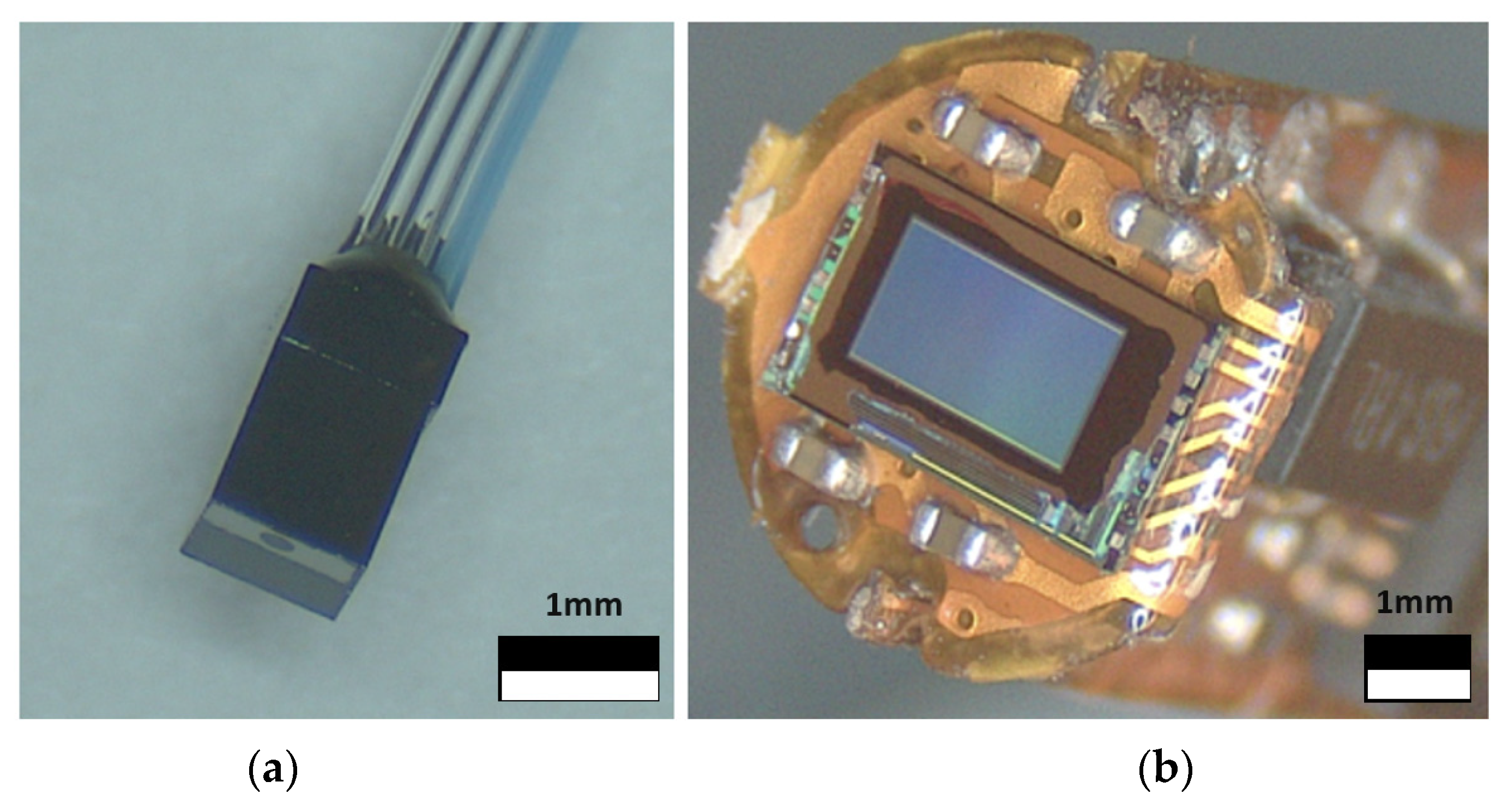
When interacting with the scintillator, electrons create a beam spot with photon emission centered at 450 nm [8]. These photons are collected either by a CMOS camera at a defined distance determined by the camera’s focal point or by a CMOS sensor without optical lenses directly attached to the scintillator. While the direct attachment generally yields superior magnetic sensitivity due to better image definition, attaching a CMOS sensor directly to probes with a diameter smaller than 5.0 mm presents challenges for existing Commercial off-the-shelf CMOS sensors [9]. When no lens system is required, the scintillator is either deposited on a glass disc or directly onto the CMOS sensor. Unless stated otherwise for a particular test, the image sensor utilized in the prototype under study is OVM6946, with package dimensions of 1.1 mm by 1.1 mm and a length of 2.4 mm. The image area measures 714 µm by 707 µm, with a pixel size of 1.75 µm by 1.75 µm, as illustrated in Figure 3a.
The image, captured by the CMOS sensor, is subsequently transmitted to a computer via differential lines for digital signal processing. Currently, a computer functions as the digital signal processor unit and computes the magnetic field based on the position and shape of the beam spot. Any deviation in the beam spot from its rest position is translated into a magnetic field measurement. To enhance magnetic resolution, the signal processing algorithm conducts centroid localization, considering both the illuminated pixel position and its intensity. Determining the optimal pixel size is challenging, as it hinges on several factors, including the beam spot size, signal-to-noise ratio of the pixel, pixel charge threshold, and quantum efficiency. Optimizing the pixel size directly impacts magnetic resolution, with smaller pixels enhancing spatial resolution up to a certain point. The beam spot dimension is of paramount importance and the optimal pixel size is directly related to its size. For the prototype imager analyzed in this study, we adopted a pixel size of 1.75 µm by 1.75 µm, which is more than 50 times smaller than the beam spot; this was empirically inferred to be around six times smaller than the minimum necessary size, and further reducing the pixel sizes did not yield better results. Signal processing may also encompass averaging several frames of the beam spot to enhance sensitivity, albeit at the expense of speed. The centroid localization is performed via k-means algorithm to determine a pixel cluster within an unlabeled multidimensional dataset [10]. In this context, the image inputted to the k-means clustering algorithm comprises the hits registered on the CMOS detector. Given that the source utilized is a Gaussian with tens of microns of spatial spread, most particles deposit charge in a primary cluster. However, the scattering of particles due to the beam interacting with the scintillator and Wehnelt cylinder leads some electrons to deposit charges away from the central cluster. The center of the cluster is determined as the statistical mean of all points belonging to a specific cluster. This process is iterated multiple times or until the center of the group shows insignificant changes between iterations [11].
3. Performance and Optimization
The continuous evolution of this magnetometer involves a series of incremental improvements aimed at enhancing its overall performance. In this section, we will describe the current state of the probe, providing detailed insights into its performance metrics and the parameters currently undergoing optimization.
The optimization of the magnetic probe presented in this work is primarily guided by its designated application, in this case, the characterization of undulators for insertion devices [12]. This specific application demands probes with a compact diameter ranging from 3.0 mm to 5.0 mm, spatial resolution of 500 μm or less, and a wide magnetic field range, capable of measuring up to 3T, all while maintaining a magnetic sensitivity of 25 μT and an accuracy of 1000 ppm for the stated range. Additionally, it is crucial for the probe to swiftly traverse through undulators, allowing for rapid characterization with a targeted minimum linear speed of 10 mm/s with 40 measurements per second [13,14,15,16].
In addressing the challenges associated with a small diameter, as illustrated in Figure 3, two strategies have been implemented. For smaller diameters where space prohibits direct sensor attachment to the scintillator, an alternative approach is adopted where a micro camera with a lens system is deployed. Conversely, when the diameter allows, a scintillator can be directly deposited onto the sensor. It has been determined that the imager can effectively incorporate pixels as large as 10 μm × 10 μm while still yielding 25 μT resolution.
The performance of the 5.0 mm diameter probe discussed in this work and depicted in Figure 4 is summarized in Table 1. Despite the outer diameter of the probe being 5.0 mm, the current CMOS sensor utilized has a circular viewing area of 4.5 mm determined by its focal distance and the construction of the probe. While the maximum magnetic field and accuracy for this application are easily attainable with the existing prototypes, the field sensitivity remains a crucial factor, currently falling short by a factor of ten from the targeted performance. Thus, ongoing improvements are imperative for this particular application.
The accelerating electric field is a very important factor for the performance of this probe, and it is mainly defined by the difference in electric potential between the cathode and the anode. Currently, the optimal voltage stands at 250 V, aimed at fulfilling the requirements of the target application for a probe featuring a channel length ranging from 350 μm to 500 μm. There are two main limitations for this parameter; higher values can cause an electric arc due to the probe’s reduced dimensions limiting the maximum voltage to 2000 V, and lower values are limited by the scintillator cross-section, with this particular scintillator reducing its efficiency exponentially under 200 V. For this application the accelerating electric field could not be too high to preserve high sensitivity while maintaining the desired dynamic range.
The LaB6 cathode maintains a minimum stable current of approximately 10 nA, equivalent to 6.25 × 10¹⁰ electrons per second. Less than 10% of these electrons successfully traverse the collimating orifice with the actual percentage depending on the position of the cathode. The spatial distribution beyond the orifice and at the scintillator/phosphor plane approximates a 2D Gaussian with a standard deviation of 20 micrometers. The accelerated electrons, depending on the operating voltage, possess energy levels ranging from 200 to 2000 eV. Considering a 250 V accelerating potential, each electron generates 2–3 scintillation photons, but only about ~5% of these photons lead to a signal (an ionization e-h pair) in the CMOS sensor [17]. We can currently reach a 1-micrometer position resolution that yields 250 µT for a 600-µm-long channel, as illustrated by Table 1, with measurements of the beam position within 25 ms time intervals. In such intervals, in theory, over 10 million ionization electrons could be measured; in practice, it saturates the sensor and has to be dimmed by a filter.
Probes with longer active channels, designed for applications demanding heightened sensitivity but with reduced dynamic range, are currently undergoing testing. Figure 5 displays the performance obtained from a 10 mm long probe capable of reaching 50 nT field sensitivity. The figure portrays the typical pattern captured by the imager, highlighting the presence of rogue pixels attributed to electron scattering. Additionally, the image underscores that a beam spot cluster can consist of hundreds of pixels. Although the beam spot hit map has a Gaussian hit distribution, in this scenario, the pixels were saturated and the centroid was computed using binary pixels, where each pixel is either on or off.
It is noteworthy that employing relatively large beam spots contributes to enhancing the probe’s sensitivity by offering more statistical data for centroid calculations. However, a trade-off is evident, as larger pixel clusters mirror the beam spot’s size, resulting in a reduction in the probe’s dynamic range; this occurs when the beam spot reaches the sensor boundary earlier in instances of large pixel clusters.
Another important optimization implemented in this probe is the distance between the electron emitter and the Wehnelt cylinder. This important parameter optimizes the beam divergence and its brightness. For this probe, the tip of the LaB6 emitter was located at 400 µm from the Wehnelt cylinder with a 150 µm aperture. This provided the best trade-off between brightness and divergence. The transmitted brightness is determined by the percentage of electrons generated by the cathode that successfully traverses the cylinder aperture before being converted into light by the scintillator.
Table 2 shows the transmitted brightness at the scintillator, with measurements within a 20% margin of error, obtained by assessing the number of photons emitted by the scintillator versus the electrons projected by the cathode. Figure 6 shows electrostatic simulations that helped to optimize the relative position of the electron emitter. For this application, the Wehnelt cylinder was kept at zero electric potential.
This probe demonstrates versatility by functioning in a cold environment, with prototype versions capable of operating while immersed in liquid nitrogen. The primary factor influencing performance is the CMOS cameras. Notably, some CMOS cameras exhibit enhanced performance when directly operated in liquid nitrogen due to reduced dark current caused by the low temperature [17]. Cold operation is facilitated by the internal hot cathode, which functions as a heater, maintaining the probe’s internals at a temperature warmer than the surrounding environment. This configuration effectively creates a reverse cryostat, akin to the operation of numerous cryogenic cameras [18,19]. No performance degradation was observed when operating at 77 K other than an increase in the cathode current due to the reduction in its internal resistance resulting from the cold environment.
While the probe operates effectively in cryogenic liquid, its prolonged functioning in such an environment, along with its resilience to multiple thermal cycles, remains uncertain.
4. Discussion
Previously, we established that the performance of the magnetic probe is intricately linked to trade-offs among key parameters, encompassing accuracy, spatial resolution, temperature range, and sensitivity. Optimizing these parameters becomes especially critical when customizing the probe for the specific application discussed in this study, where a small diameter is essential for the probe to be viable. In the context of our focus application, the primary hurdle lies in achieving the targeted sensitivity while maintaining the desired dynamic range.
To address this challenge, an array of proactive strategies is actively being pursued. These strategies include the implementation of advanced signal processing techniques, the exploration of alternative scintillator types, and the integration of electrostatic deflecting plates. The collective objective of these endeavors is to elevate the sensitivity of the prototype and align it with the specified target of 25 µT.
The primary challenge arises from the minimal detectable displacement of the electron beam by the imager. Factors contributing to this measurement error include the suboptimal scintillator material for detecting low-energy electrons, which currently limits the usable energy range. We are actively exploring alternative scintillating materials capable of operating effectively with lower energy electrons [18]. Alternatively, in the long term, we aim to develop a custom-made CMOS imager optimized for direct electron detection [20], drawing upon the expertise we have gained thus far. This image will have its pixel size optimized for this application and its imaging area designed to offer the maximum possible active area in the available space. It also will be back-illuminated with a thinned window to allow for the efficient collection of low-energy electrons.
The utilization of lower-energy electrons introduces a new challenge, it further reduces the dynamic range of the probe due to excessive beam deflection. To address this issue, our strategy involves the integration of deflecting electrostatic rings [20,21]. This approach aims to counteract magnetic deflection, ensuring efficacy with lower-energy electrons while simultaneously achieving the targeted dynamic range and sensitivity. This would be achieved by a feedback system that constantly compensates for the magnetic field.
Another solution we are pursuing is to enhance sensitivity via the replacement of the monolithic scintillator. The current scintillator exhibits excessive light bleeding, which compromises the capacity of the signal processing algorithm to resolve the centroid. To address this, a pixelated scintillator is in development. With a sensor featuring 5 μm by 5 μm pixels, the light spreads over 100 pixels, translating to ~100,000 ionization electrons. This surpasses the typical pixel charge capacity (well depth), necessitating light attenuation, ideally around 1–10% transparency. A semi-transparent deposited thin film can easily achieve this requirement.
In this system, the position resolution primarily hinges on the beam width at the phosphor plane (larger than the light guides and sensor pixels) and the quantity of measured ionization electron quanta. With a presumed 95% light attenuation, we anticipate measuring approximately half a million ionization electrons. This would result in a resolution of around 20 μm/sqrt (5 × 10⁶), theoretically making it possible to determine the beam spot center with 0.03 μm within a 25 ms time interval. Achieving this level of resolution allows our current 800 μm probe, as presented in Table 1, to exhibit a sensitivity of 0.5 µT, while the 400 μm probe demonstrates a sensitivity of 20 µT, within the applicable range for this particular application. Determining the beam position involves the centroid calculation of pixels with a collected charge above a noise threshold. Sensor noise is not a significant limitation, given that the collected charges in illuminated pixels far exceed typical sensor noise. The primary systematic error is expected from the square light guides and sensor pixels.
The centroid finding algorithm can be refined through simulations and/or direct measurements in a known varying magnetic field. At present, this critical function is executed by a conventional computer, where the emphasis lies on sustaining real-time operation, thus necessitating a streamlined algorithm that avoids computationally intensive processes. A pivotal shift is underway as we migrate from a computer-based infrastructure to a Field Programmable Gate Array (FPGA) device. By leveraging FPGA’s parallel processing power, we anticipate a profound boost in computational efficiency, paving the way for more intricate and resource-demanding image processing algorithms [22,23].
One of the main changes in the algorithm is the increased use of averaging within each image frame. This strategic upgrade not only enhances the efficiency of the image processing algorithm, but also aligns with our objective of advancing the overall capabilities of the probe for more sophisticated and nuanced magnetic field measurements. In a single frame, the probe can capture a cluster of many pixels enabling the determination of the beam’s position and, consequently, the incident magnetic field. Averaging an ‘n’ number of pixels per frame leads to an enhanced signal-to-noise ratio. The frame image processing addresses random noise, assuming that cluster noise is genuinely random. This approach ensures that fluctuations (noise) in the image gradually smooth out as more pixels are averaged. Generally, the magnitude of fluctuations diminishes by the square root of the number of averaged pixels. The relationship between performance improvement and the number of samples can be expressed by
with SNRn being the average signal-to-noise ratio, n the number of pixels being averaged, and SNRi initial signal-to-noise ratio (SNRi). This strategy alone may get the performance of this probe to the desired sensitivity while maintaining the speed requirements of 40 frames per second, with each frame being a magnetic measurement the algorithm has to take 25 milliseconds to converge for each measurement.
The FPGA implementation of the complete system is currently in progress, and it will enable this magnetic probe to function as a standalone system. In addition to centroid localization and data handling, it will control the electrostatic deflection plates designed to maintain the beam spot within the desired range. As illustrated by Figure 7, data originating from the probe arrives from the CMOS camera in a single LVDS (Low Voltage Differential Signal) line, and it is immediately decoded by the CDR (Clock and Data Recovery) block and is then formatted in a frame.
The framed data is subsequently processed by the DSP block, which calculates the magnetic field from the raw pixel data and forwards it to the IPBus [24]. This system then makes the information accessible for broadcast through the Ethernet. External commands can also be received to configure the camera via Ethernet.
In concluding the discussion on the capabilities, improvements, and future applications of this probe, it is important to highlight an ongoing development: the prototype featuring an optical fiber bundle. This advancement represents a significant stride towards enhancing the versatility and robustness of the magnetometer in challenging environments. This fiber bundle, comprising 3 µm fibers, will replace the conventional detector and be strategically positioned at the current probe’s imager location. In this configuration, the electron beam will illuminate a scintillator affixed to the optical fiber bundle. The resulting optical pattern will be transmitted to the imager affixed to the far end of the bundle. Subsequently, a signal processing algorithm will be applied to compute the centroid of the beam. It is important to note that, when compared to an imager integrated inside the probe as presented in this article, the fiber bundle has limitations, particularly in terms of lower resolution due to the restricted number of fibers. Nevertheless, the fiber bundle offers increased robustness, enabling operation in high radiation settings such as fusion experiments and at deep cryogenic temperatures such as liquid helium, conditions that are very challenging for traditional image sensors.
The combination of a number of these strategies holds the promise of significantly augmenting the magnetic sensitivity of the probe, ultimately aligning it more closely with the requirements of our target application.
5. Conclusions
In this paper, we have discussed the study of the magnetometer prototype Digital Miniature Cathode Ray, highlighting its target application for the characterization of light source undulators. By harnessing a charged particle beam and digital imaging techniques, this device addresses a variety of the limitations inherent in traditional magnetic probes.
Special focus was placed on the design, construction, and characterization of the five-millimeter prototype, tailored specifically for the characterizing undulators. While most specs of the probe reached the desired goals, the prototype’s sensitivity requires additional refinement to meet the more extreme cases that this application demands. Efforts to improve the probe performance are underway—including signal processing enhancements, exploration of alternative scintillator materials, and integration of electrostatic deflecting plates—are poised to further improve the magnetometer’s sensitivity. Future developments, such as the implementation of a custom-made CMOS imager optimized for direct electron detection and the use of optical fiber bundles for enhanced robustness in extreme environments, hold promise for expanding the magnetometer’s applications even further.
In a broader context, this research significantly advances magnetic measurement technology, with implications spanning scientific, medical, and industrial domains. The innovative features of this magnetometer offer promising avenues for progress across various fields, solidifying its position as a valuable asset in the ongoing evolution of measurement technologies.
Author Contributions
Conceptualization, M.T.; methodology, M.T. and G.W.; validation, M.T. and G.W.; formal analysis, M.T., A.G. and G.W.; investigation, M.T., R.C. and G.W.; data curation, M.T.; writing—original draft preparation, M.T.; writing—review and editing M.T., G.W., A.G. and R.C.; project administration, M.T.; funding acquisition, M.T. All authors have read and agreed to the published version of the manuscript.
Funding
This research was performed at Lawrence Berkeley National Laboratory under UC-DOE contract DE-AC02-05CH11231 funded by the Department of Energy, Office of Science, Early Carrier Research Program DE-FOA-0002563.
Data Availability Statement
The raw data supporting the conclusions of this article will be made available by the authors on request.
Conflicts of Interest
The authors declare no conflict of interest.
References
- Kawai, J.; Miyamoto, M.; Kawabata, M.; Nosé, M.; Haruta, Y.; Uehara, G. Characterization and demonstration results of a SQUID magnetometer system developed for geomagnetic field measurements. Supercond. Sci. Technol. 2017, 30, 084002. [Google Scholar] [CrossRef]
- Bottura, L.a.H.K. Field Measurements; European Organization for Nuclear Research (CERN): Geneva, Switzerland, 2002. [Google Scholar]
- Ramsden, E. Hall-Effect Sensors: Theory and Application; Elsevier: Amsterdam, The Netherlands, 2011. [Google Scholar]
- Temnykh, A.; Levashov, Y.; Wolf, Z. A study of undulator magnets characterization using the vibrating wire technique. Nucl. Instrum. Methods Phys. Res. 2010, 622, 650–656. [Google Scholar] [CrossRef]
- Zhu, K.; Kiourti, A. A Review of Magnetic Field Emissions From the Human Body: Sources, Sensors, and Uses. IEEE Open J. Antennas Propag. 2022, 3, 732–744. [Google Scholar] [CrossRef]
- Wheeler, T.R.H.; Clark, M.G. CRT Technology; Springer: Berlin/Heidelberg, Germany, 1992; pp. 221–256. [Google Scholar]
- Sewell, P.B. General Guidelines for Operating ES-423R LaB6 Cathodes; Kimball Physics Inc.: Wilton, NH, USA, 1991. [Google Scholar]
- Yen, W.M.; Shionoya, S.; Yamamoto, H. Phosphor Handbook, 2nd ed.; CRC Press; Taylor & Francis Group: Boca Raton, FL, USA, 2007. [Google Scholar]
- Hoffman, A.; Loose, M.; Suntharalingam, V. CMOS detector technology. Experim. Astron. 2006, 19, 111–134. [Google Scholar] [CrossRef]
- Na, S.; Xumin, L.; Yong, G. Research on k-means Clustering Algorithm: An Improved k-means Clustering Algorithm. In Proceedings of the Third International Symposium on Intelligent Information Technology and Security Informatics, Ji’an, China, 2–4 April 2010; pp. 63–67. [Google Scholar] [CrossRef]
- Chen, C.W.; Luo, J.; Parker, K.J. Image segmentation via adaptive K-mean clustering and knowledge-based morphological operations with biomedical applications. IEEE Trans. Image Process. 1998, 7, 1673–1683. [Google Scholar] [CrossRef] [PubMed]
- Baader, J.E.; Abeghyan, S.; Casalbuoni, D.C.S.; Marchetti, B.; Yakopov, M.; Eckoldt, H.J.; Hauberg, A.; Lederer, S.; Lilje, L.; Wohlenberg, T.; et al. SUNDAE2 at EuXFEL: A Test Stand to Characterize the Magnetic Field of Superconducting Undulators. In Proceedings of the 13th International Particle Accelerator Conference, Bangkok, Thailand, 12–17 June 2022. [Google Scholar]
- Wei, J.; Li, X.Y.; Chen, Z.; Zhang, X.X. Development and magnetic field measurement of a 0.5-m-long superconducting undulator at IHEP. J. Synchrotron Radiat. 2022, 29, 997–1003. [Google Scholar] [CrossRef]
- Calvi, M.; Camenzuli, C.; Ganter, R.; Sammut, N.; Schmidt, T. Magnetic assessment and modelling of the Aramis undulator beamline. J. Synchrotron Radiat. 2018, 25, 686–705. [Google Scholar] [CrossRef] [PubMed]
- Gerstl, S.; Boffo, C.; Casalbuoni, S.; Gerhard, T.; Glamann, N.; Grau, A.; Holubek, T.; Jauregui, D.D.; Turenne, M.; Voutta, R. First Characterization of a Superconducting Undulator Mockup with the CASPER II Magnetic Measurement System. In Proceedings of the IPAC 2015, Richmond, VA, USA, 3–8 May 2015. [Google Scholar] [CrossRef]
- Tanaka, T.; Tsuru, T.R. Magnetic characterization for cryogenic permanent-magnet undulators: A first result. J. Synchrotron Radiat. 2007, 14, 416–420. [Google Scholar] [CrossRef]
- Janesick, J.R.; Elliott, T.; Collins, S.; Blouke, M.M.; Freeman, J. Scientific charge-coupled devices. Opt. Eng. 1987, 26, 692–714. [Google Scholar] [CrossRef]
- Yanagida, T. Inorganic scintillating materials and scintillation detectors. Proc. Jpn. Acad. 2018, 94, 75–97. [Google Scholar] [CrossRef] [PubMed]
- McConkey, N.; Spooner, N.; Thiesse, M.; Wallbank, M.; Warburton, T. Cryogenic CMOS cameras for high voltage monitoring in liquid argon. J. Instrum. 2017, 12, P03014. [Google Scholar] [CrossRef]
- Bheesette, S.; Turqueti, M. Simulation Studies for an Electron Gun Based Magnetic Probe. IEEE Trans. Nucl. Sci. 2023, 70, 177–188. [Google Scholar] [CrossRef]
- Baumgärtel, C.; Smith, R.T.; Maher, S. Accurately predicting electron beam deflections in fringing fields of a solenoid. Sci. Rep. 2020, 10, 10903. [Google Scholar] [CrossRef] [PubMed]
- Li, Y.; Yao, Q.; Tian, B.; Xu, W. Fast double-parallel image processing based on FPGA. In Proceedings of the 2011 IEEE International Conference on Vehicular Electronics and Safety, Beijing, China, 10–12 July 2011. [Google Scholar]
- Siddiqui, F.; Amiri, S.; Minhas, U.; Deng, T.; Woods, R.; Rafferty, K.; Crookes, D. FPGA-Based Processor Acceleration for Image Processing Applications. J. Imaging 2019, 5, 16. [Google Scholar] [CrossRef] [PubMed]
- Kunihiro, T.; Nagashima, K.; Takayanagi, I.; Nakamura, J.; Kosaka, K.; Yurimoto, H. Noise characteristics of stacked CMOS active pixel sensor for charged particles. NIST 2001, 470, 512–519. [Google Scholar] [CrossRef]
Figure 1.
This figure illustrates the basic design of the magnetic probe that is divided into two basic blocks; the electron accelerator on the left, and the imager on the right. The electron beam originated in the LaB6 based cathode (dashed line), it is accelerated towards the scintillator, and the resulting beam spot is imaged by the CMOS camera. This picture is not to scale, and some dimensions are exaggerated to better illustrate its working principles.

Figure 2.
The electron gun assembly contains three basic elements; (a) the electron emitter, (b) the Wehnelt cylinder, and (c) the anode.
Figure 2.
The electron gun assembly contains three basic elements; (a) the electron emitter, (b) the Wehnelt cylinder, and (c) the anode.

Figure 3.
(a) OVM6946 CMOS sensor with lens assembly, and (b) CMOS sensor directly coupled to the scintillator.
Figure 3.
(a) OVM6946 CMOS sensor with lens assembly, and (b) CMOS sensor directly coupled to the scintillator.

Figure 4.
Depiction of a typical magnetic probe undergoing testing. The outer diameter measures 5.0 mm and the main body 6.5 mm. The 1.0 mm copper tabs are built-in to connect the Wehlnet cylinder. The CMOS sensor attached to this prototype is the OVM6946 with square pixels measuring 1.75 µm by 1.75 µm.

Figure 5.
Four frames at different magnetic fields for a probe with an active channel of 10 mm. The centroids marked in each cluster were calculated using k-means. The centroid localization algorithm used binary pixels for this calculation.
Figure 5.
Four frames at different magnetic fields for a probe with an active channel of 10 mm. The centroids marked in each cluster were calculated using k-means. The centroid localization algorithm used binary pixels for this calculation.

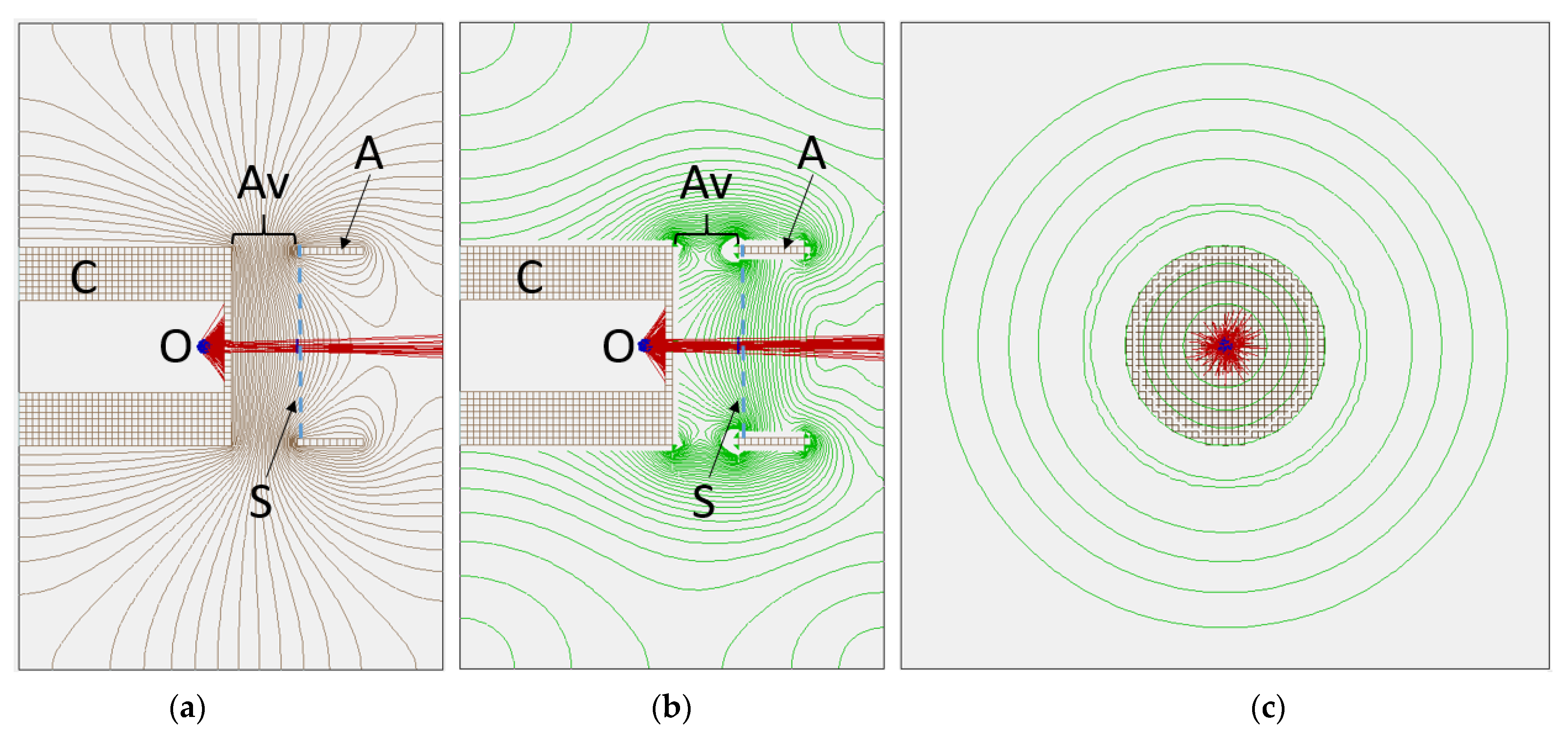
Figure 6.
Illustrating the electrostatic simulation of the probe, with key elements designated as follows: “O” denotes the origin of the electron beam, “S” represents the scintillator, “C” signifies the Wehlnet cylinder, “A” denotes the anode, and “Av” encompasses the active volume of the probe spanning the distance between the anode and the Wehlnet cylinder, set to 600 μm. In detail, (a) portrays the vertical cross-section of the electric field equipotential, (b) presents the vertical cross-section of the gradient lines, and (c) illustrates the horizontal cross-section of the gradient lines. The interactions between electrons originating at the cathode are depicted in blue, and the scintillator is highlighted, with the electron beam shown in red.

Figure 7.
The block diagram depicts the implementation of the probe as a system-on-a-chip within the FPGA.
Figure 7.
The block diagram depicts the implementation of the probe as a system-on-a-chip within the FPGA.


Table 1.
The results below show the current performance of a 5.0 mm diameter probe, with 250 V electrostatic acceleration averaging 24 frames with each centroid acquired every 30 milliseconds. The utilized cathode was LaB6 and the imager was the OVM6946.
Table 1.
The results below show the current performance of a 5.0 mm diameter probe, with 250 V electrostatic acceleration averaging 24 frames with each centroid acquired every 30 milliseconds. The utilized cathode was LaB6 and the imager was the OVM6946.
| Spatial Resolution (µm) | Accuracy (ppm) | Field Sensitivity (µT) | Maximum Field (T) |
|---|---|---|---|
| 400 | 240 * | 600 | 3.00 * |
| 600 | 94 | 250 | 1.33 |
| 800 | 75 | 150 | 0.75 |
* This particular value was reached by simulation and confirmed by extrapolating test results. We currently have the capability to test articles only up to 1.5T; The field sensitivity has a margin of error of ±2% while the accuracy ± 1.5%.
Table 2.
The results below show the electron beam divergence and electron transmission rate dependence on the electron emitter distance from the Wehnelt cylinder aperture to the cathode. The cylinder potential was set to zero, and the acceleration field to 250 V.
Table 2.
The results below show the electron beam divergence and electron transmission rate dependence on the electron emitter distance from the Wehnelt cylinder aperture to the cathode. The cylinder potential was set to zero, and the acceleration field to 250 V.
| Distance (µm) | Transmitted Brightness (%) | Divergence Angle (°) |
|---|---|---|
| 200 | 7.4 | 2.2 |
| 400 | 3.0 | 1.7 |
| 600 | 1.9 | 1.4 |
| 800 | 0.9 | 1.0 |
Disclaimer/Publisher’s Note: The statements, opinions and data contained in all publications are solely those of the individual author(s) and contributor(s) and not of MDPI and/or the editor(s). MDPI and/or the editor(s) disclaim responsibility for any injury to people or property resulting from any ideas, methods, instructions or products referred to in the content. |
© 2024 by the authors. Licensee MDPI, Basel, Switzerland. This article is an open access article distributed under the terms and conditions of the Creative Commons Attribution (CC BY) license (https://creativecommons.org/licenses/by/4.0/).
Share and Cite
MDPI and ACS Style
Turqueti, M.; Wagner, G.; Goldschmidt, A.; Carney, R. Digital Miniature Cathode Ray Magnetometer. Instruments 2024, 8, 29. https://0-doi-org.brum.beds.ac.uk/10.3390/instruments8020029
AMA Style
Turqueti M, Wagner G, Goldschmidt A, Carney R. Digital Miniature Cathode Ray Magnetometer. Instruments. 2024; 8(2):29. https://0-doi-org.brum.beds.ac.uk/10.3390/instruments8020029
Chicago/Turabian StyleTurqueti, Marcos, Gustav Wagner, Azriel Goldschmidt, and Rebecca Carney. 2024. "Digital Miniature Cathode Ray Magnetometer" Instruments 8, no. 2: 29. https://0-doi-org.brum.beds.ac.uk/10.3390/instruments8020029