
A Hybrid Scheme for TX I/Q Imbalance Self-Calibration in a Direct-Conversion Transceiver


1
School of Aeronautics and Astronautics, Zhejiang University, Hangzhou 310030, China
2
China United Network Communications Co., Ltd., Jiangsu Branch, Nanjing 210019, China
*
Author to whom correspondence should be addressed.
Electronics 2024, 13(9), 1653; https://0-doi-org.brum.beds.ac.uk/10.3390/electronics13091653
Submission received: 6 April 2024
/
Revised: 22 April 2024
/
Accepted: 24 April 2024
/
Published: 25 April 2024
(This article belongs to the Section Circuit and Signal Processing)
Abstract
:A generic transmitter (TX) I/Q imbalance self-calibration method, which was designed based on a hybrid analog and digital structure, is proposed in this paper. The whole calibration scheme was implemented using low-complexity digital–analog circuits based on a zero-force feedback loop. In order to eliminate the negative effect of local oscillator (LO) harmonics on the calibration, we used a variable-delay line (VDL) in the analog domain instead of the digital phase compensator. The prototype chip was fabricated within a 0.2∼5.0 GHz direct-conversion transmitter in a 65 nm CMOS process, and measurements found an image rejection ratio (IRR) of 65 dBc.
1. Introduction
The direct-conversion scheme is widely used in modern radio frequency (RF) integrated transceivers because of its low cost, low complexity and reconfigurable architecture [1,2]. However, the I/Q imbalance is an unavoidable impairment of direct-conversion transceivers due to manufacturing defects, such as layout mismatches [3]. Studies [4,5] have shown that the performance of multi-carrier, multi-antenna modulation systems, such as LTE, is notably sensitive to I/Q imbalance because the image frequency component overlaps the desired signal of the corresponding sub-carriers, which decreases the SNR of the desired signal [6,7,8]. As a critical criterion of I/Q imbalance, the image rejection ratio (IRR) is only 25–40 dBc in direct-conversion transceivers without I/Q compensation. However, a stringent IRR (more than 60 dBc) is desired in many modulation systems [1].
To improve the IRR, many analog solutions, such as I/Q double-balanced passive mixers and I/Q RF variable gain amplifiers (VGAs), have been suggested [9,10]. However, these kinds of schemes require a large area and high power dissipation. Furthermore, some improved analog solutions were suggested later, such as the local oscillator (LO) I/Q imbalance cancellation circuits [11,12,13].
On the other hand, digital methods were also widely proposed over the years. The digital I/Q imbalance calibration schemes are mainly divided into blind methods and training sequence methods, according to whether data assistance is required during the calibration. Because the blind method uses only the inherent characteristics of the received signals to estimate the I/Q imbalance, it is widely used for tracking calibration, and the system does not need to stop its normal operation to enter the calibration process. However, in order to extract the inherent characteristics of the signals, the blind method requires high-complexity calculation blocks, thus usually requiring external digital signal processing (DSP) for the calibration of the whole system [14,15,16]. On the other hand, training sequence methods are easier to implement, and are widely used for power-on calibration (self-calibration) since they can implement a high-precision I/Q imbalance estimation by sending a designed training sequence [17,18,19]. Furthermore, any training sequence method for a frequency-independent I/Q imbalance calibration can be extended to calibrate a frequency-dependent I/Q imbalance by utilizing a finite-impulse response (FIR) filter in the system, since the frequency-dependent I/Q imbalance can be further compensated by changing the tap coefficient of the FIR [20,21].
In order to provide high-performance I/Q imbalance calibration and avoid complicated algorithms, a hybrid (digital–analog) I/Q calibration scheme with sign detection only is proposed in [22], where the I/Q imbalance model is simplified by a Taylor series to obtain a convenient scheme. However, it was not adopted in the transmitter (TX) and needs many cycles to converge. Another hybrid approach is presented in [23], where the IRR after calibration is 53 dBc with a 2-bit ADC. It can be seen that the above scheme is not suitable for transceivers due to its low resolution step of phase/amplitude adjustment.
In this paper, we propose a generic digital–analog hybrid TX I/Q calibration scheme for transceivers. On the one hand, to avoid complex algorithms, such as MMSE, we split the calibration of the I/Q imbalance into two parts, where both were single-variable negative-feedback systems and based on a phase compensation parameter and an amplitude compensation parameter. On the other hand, in order to eliminate the negative effect of LO high-order harmonics on the digital I/Q imbalance estimation, we optimized the digital calibration scheme by using a variable-delay line (VDL) in the analog domain to achieve a variable phase adjustment, which could improve the IRR performance of the whole calibration. The rest of this paper is organized as follows: Section 2 illustrates the whole I/Q imbalance calibration scheme in our transceiver. The I/Q imbalance compensation method and its improvement are discussed in Section 3. In Section 4, the simulation and experimental results are presented. Finally, conclusions are drawn in Section 5.
2. I/Q Imbalance Calibration Scheme
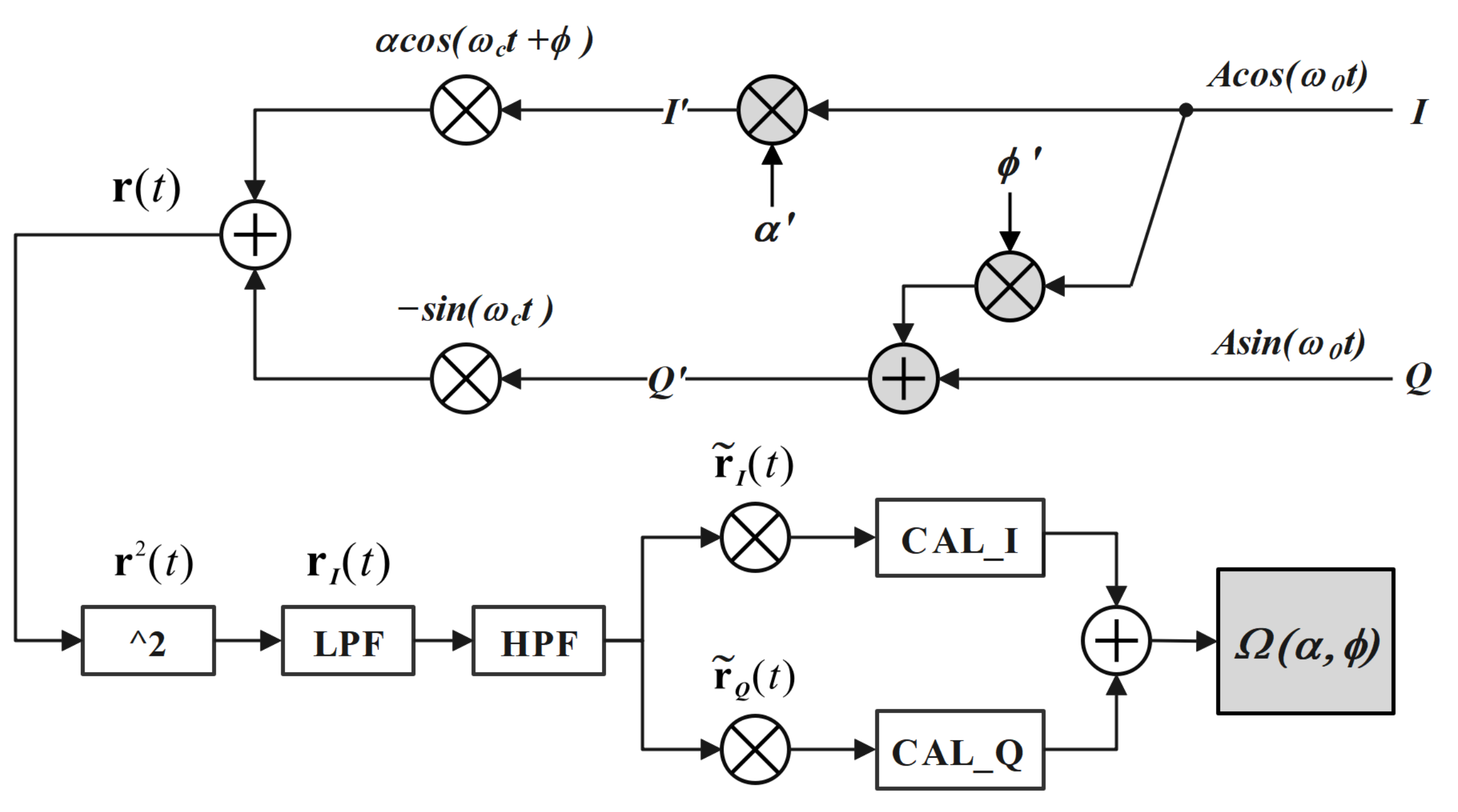
The direct-conversion transceiver consists of two independent local oscillators (LOs), namely, the LOs of the transmitter (TX LO) and receiver (RX LO), which can operate at different carrier frequencies simultaneously. In fact, due to the wide use of DSPs, it has become easier to build RX IQ imbalance schemes within a DSP. However, this kind of scheme is not robust for TX I/Q calibration because the performance in a TX is strongly dependent on RX calibration results [18,24]. To overcome the TX I/Q imbalance issue, a calibration scheme in a direct-conversion transceiver is shown in Figure 1. In addition to some necessary components, a low-cost TX I/Q imbalance compensation block and a low-cost I/Q imbalance estimation block were integrated into the digital front end. Furthermore, a squaring circuit and a variable-delay line (VDL) were integrated into the analog domain [25,26].
The TX digital domain is mainly composed of the direct digital synthesizer (DDS) and I/Q imbalance compensation block. The DDS generates a sine wave calibration signal with the specific frequency we need, while the I/Q imbalance compensation block uses the compensation parameters obtained by the I/Q imbalance estimation block to compensate for the calibration signal. The digital signal is transmitted into digital-to-analog converters (DACs ), filtered by LPF and then up-mixed with the TX LO. The VDL was inserted in the TX LO path of the mixer to compensate for the phase mismatch of the TX LO, while the compensating parameter was also given by the I/Q imbalance estimation block.
Unlike the normal signal path, the TX RF signal is transferred into the RX analog front end through an internal loop-back path during calibration. When performing TX I/Q calibration, the Q path is set to zero. Different from the most used loop-back methods proposed in [18,24], in order to eliminate the extra I/Q imbalance caused by the RX LO, our loop-back signal was squared by the squaring circuit ( in Figure 1) and directly output into the low-pass filter (LPF) in the I path without passing through the RX LO. Then, the squared signal was filtered by the LPF, converted by the analog-to-digital converter (ADC) and output into the digital domain. To avoid the overflow in ADC, a high-pass filter (HPF) was adopted to remove the large DC component caused by the squaring circuit. When the I/Q calibration is working, the digital signal first passes through the TX I/Q imbalance compensation block, and then passes through a numerically controlled oscillator (NCO), which provides the complex down-conversion with the specific frequency we need. Finally, the signal is transferred into the I/Q imbalance estimation block for calculation to achieve the whole TX I/Q calibration.
3. Model Analysis and Compensation Method
3.1. Analysis of the Digital I/Q Calibration Model
When the I/Q calibration scheme proposed in Section 2 works, two parameters, namely, and , provided by the I/Q estimation block (CAL_I and CAL_Q in Figure 2) are used to compensate for the TX baseband signals before the TX LO. Then, the RF signal from the TX LO is processed by the squaring circuit, filters, NCO and the I/Q imbalance estimation block in sequence. Based on the whole calibration system, we finally obtain a binary function , which can reflect the quantified relation between the image rejection and I/Q estimation parameters and . The whole calibration process is aimed at improving the IRR by approaching the minimum of , which is based on the negative feedback iteration between , and .
Figure 2 shows the digital calibration model in the proposed architecture. We assume that the TX ideal baseband signals are and . The carrier frequency of the TX LO is , the amplitude mismatch of which is and the phase mismatch of which is . Therefore, the TX RF signal can be derived to obtain
After passes through the squaring circuit and the LPF, it is output into the I branch of the RX. We use and to represent the signal after the squaring and the signal after low-pass filtering, respectively. By adopting the double-angle formula, can be derived to obtain
After the low-pass filtering, the higher-order components of the sum containing and in the above expression are filtered. Therefore, can be derived to obtain
Equation (3) contains a DC component with a size of . The amplitude of the DC component is even larger than the amplitude of main signals, which would cause an unexpected overflow of the quantization block in the ADC. Therefore, an HPF block was introduced to eliminate the DC component. It should be noted that we need to consider the phase delay in the path. Assume that the phase delay in the path is , and the above signals are complexly mixed with orthogonal signals with the frequency of in the digital domain. After the digital demodulation, the I branch signal and the Q branch signal can be calculated as follows:
The signals after the digital demodulation are transmitted into the I/Q imbalance estimation block to calculate the I/Q imbalance compensation parameters. It can be observed that the components containing and in Equations (4) and (5) are ideal sine waves. Therefore, during the I/Q imbalance estimation, and are, first, periodic-averaged to eliminate the terms containing ideal sine waves. Subsequently, by calculating the sum of the squares of and , the binary function can be derived to obtain
where denotes the mathematical expectation. Calculations show that if and only if the amplitude mismatch and the phase mismatch , the binary function reaches the minimum value 0. Therefore, can gradually approach zero by constantly adjusting the compensation parameters and . When is iterated to a minimum value, the and are taken as the optimal compensation values.
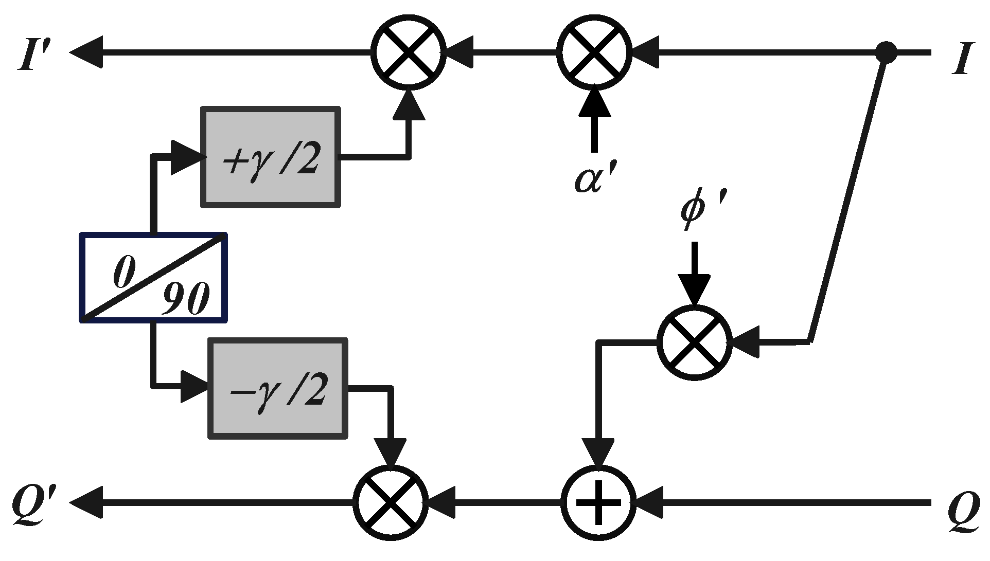
3.2. The Hybrid I/Q Compensation Method
The I/Q calibration scheme proposed in Section 3.1 can achieve a good calibration performance under the assumption of ideal analog circuits, but the performance becomes worse when suffering from the impairment of the TX LO. In fact, from the perspective of spectral analysis, the main idea of the proposed digital scheme is to obtain the frequency component at by calculating the product of the positive main signal and the negative image signal in the time domain, which can be regarded as the sum in the frequency domain. Then, the signal with a frequency of can be calculated by subsequent algorithms to obtain the function , which reflects the image rejection of the I/Q imbalance.
However, when the higher-order harmonics of the LO signal exist (take the third-order harmonics as an example), both of the main signal and image signal in the baseband will be up-mixed by the third-order harmonics of the LO. Therefore, not only the sum of and but also the sum of and will contain a frequency component at (see Figure 3). These spectral components at will overlap, which is harmful to the function proposed in Section 3.1, and thus, the digital I/Q imbalance calibration will be disturbed. The phase imbalance of caused by the TX LO can be easily rejected by the digital phase compensation parameter, but this phase imbalance obviously becomes in the third-order harmonic of the TX LO, which is unable to be compensated by the digital phase compensation parameter .
Because of the reasons given above, we inserted the variable-delay line (VDL), which consisted of the 9-bit trim capacitor, into the TX LO path of the mixer. The VDL was placed after the TX LO but before the analog mixer so it can directly adjust the delay in the I and Q paths of the LO (but not the phase), and the same delay in the LO harmonics can be adjust simultaneously (see Figure 4). In particular, the proposed VDL covers a ±7.5° range with a 0.03° step when the TX LO works at 1 GHz, which is wide enough for the possibility of phase mismatch and accurate enough for the phase adjustment. The 9-bit signed parameter of the VDL is given by the digital I/Q imbalance estimation block so that and can determine whether to apply the I or Q path in the VDL (see Figure 5). It should be noted that the amplitude compensator keeps working at the same time when the VDL is used, even if the phase compensator in the digital domain can be used for a two-stage phase compensation if necessary. In general, the proposed scheme in this section is aimed at the IRR improvement based on the joint of analog compensation and digital estimation with a low-complexity design.
4. Simulation and Experimental Results
In order to verify the schemes proposed in Section 3.1 and Section 3.2 (named schemes A and B, respectively), we set up a MATLAB platform for the simulation. The TX baseband transmitted the single-tone signal with a frequency of 3.9 MHz, and the TX LO frequency was 100 MHz. At the same time, this simulation added the amplitude imbalance parameter and the phase imbalance parameter. Furthermore, we added a third-order harmonic of the TX LO, the amplitude of which was one-quarter of the TX LO signal. Figure 6 shows the spectrum of the TX RF signal. At the image frequency of 96.1 MHz, the green asterisk represents the image amplitude without I/Q compensation, the amplitude of which was −35 dBFS. The purple asterisk represents the image rejection after using the digital scheme, the amplitude of which was −65 dBFS. As a contrast, the image rejection reached −107 dBFS after using the hybrid scheme. Figure 7 shows the spectrum of the TX RF signal after passing through the squaring circuit. It can be observed that although the digital scheme had a rejection frequency of 7.8 MHz, it was far from achieving the performance of the the hybrid scheme. In general, based on Figure 6 and Figure 7, it was shown that the proposed hybrid scheme had a considerable improvement in the I/Q imbalance compensation compared with the digital scheme when the high-order harmonics of the TX LO existed.
An experimental platform was built to verify the I/Q imbalance calibration scheme proposed in this paper (see Figure 8), which mainly included a host computer, RF signal generator, Xilinx’s FPGA (ZC706), KEYSIGHT’s PXA signal analyzer (N9030B) and direct-conversion transceiver chip with the proposed I/Q calibration scheme in it. For the self-calibration scheme of the chip, the calibration only works before the system normal operation. When the chip is powered on, the RF signal generator output the reference signal for the PLL of the chip. The FPGA and transceiver chip were controlled by the host computer to generate the TX baseband signals and start the I/Q calibration, respectively. In the end, the TX RF spectrum, which shows the IRR performance, can be seen on the signal analyzer. We conducted experiments on single-tone signals and wideband signals:
- The FPGA sent single-tone signals with the frequency of 5.28 MHz and the amplitude of −9 dBFS. The TX LO frequency was configured to 2.9 GHz.
- The FPGA sent a wideband signal with a modulation mode of quadrature phase-shift keying (QPSK), which was configured with a roll-off factor of 0.5, a symbol transmission rate of 8 Msps and an amplitude of −15 dBFS. The TX LO frequency was configured to 3 GHz.
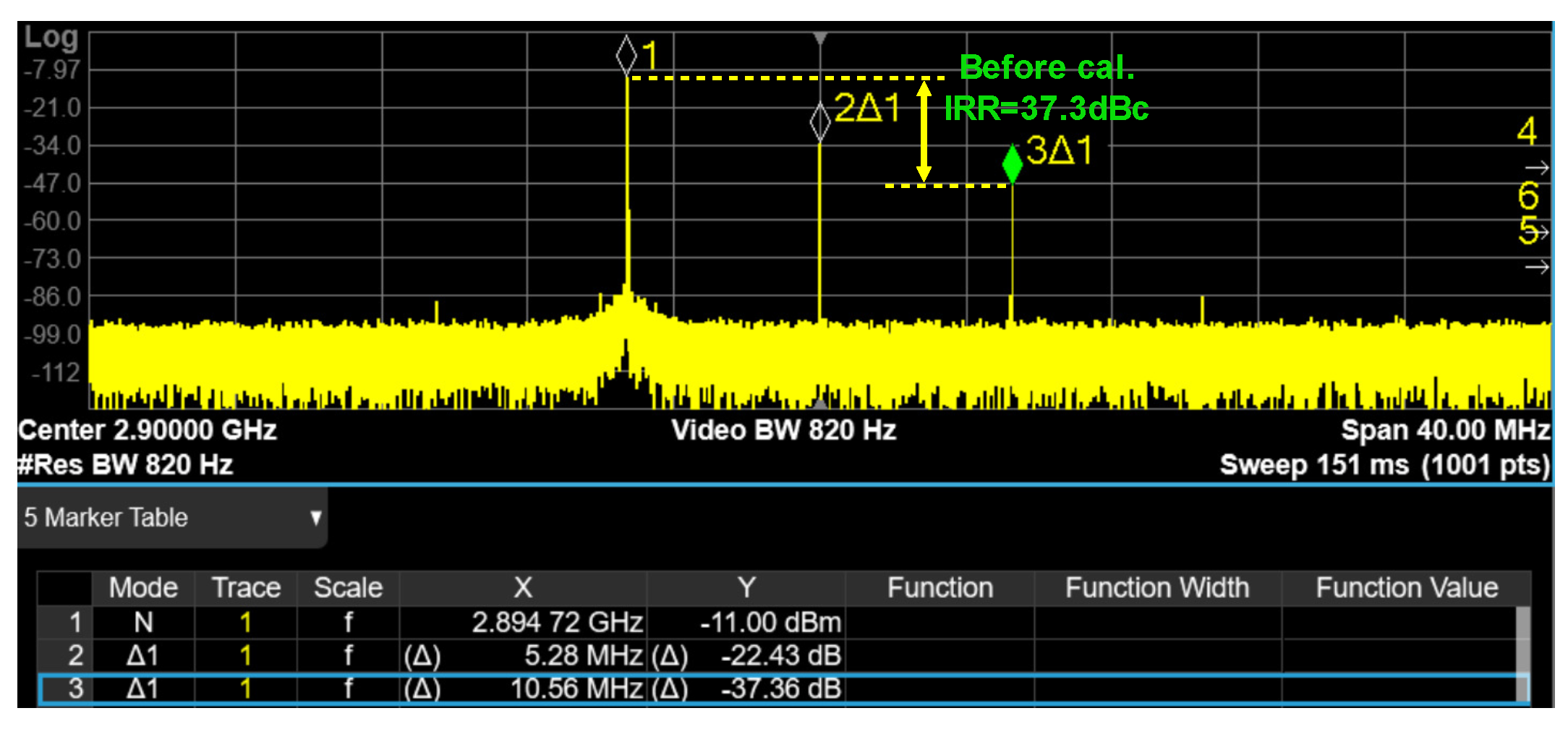
Figure 9, Figure 10 and Figure 11 show the TX RF spectrum when the FPGA sent the single-tone signal. Among them, Figure 9 exhibits the TX RF spectrum before the I/Q calibration, while Figure 10 and Figure 11 show the I/Q calibration results of the digital scheme and the proposed hybrid scheme, respectively.
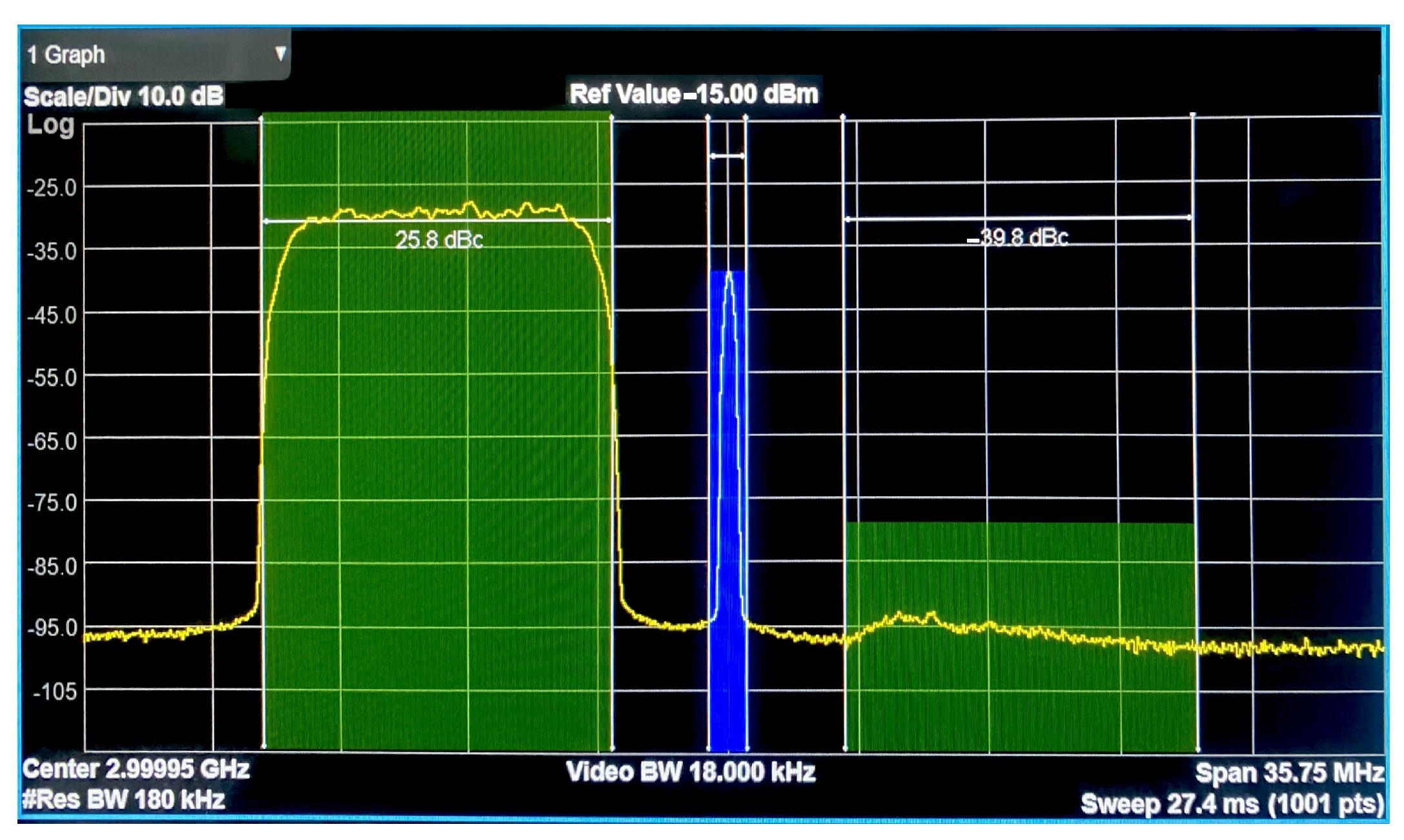
Figure 12 and Figure 13 also exhibit the I/Q calibration results of the digital scheme and the proposed hybrid scheme, respectively, while using the wideband signal as a TX baseband source. It can be observed that the IRR of the single-tone signal was improved from 37.3 dBc to 54.1 dBc/70.5 dBc (by each scheme, respectively), and no matter what the single-tone or wideband signal was, the proposed scheme had at least a 10 dB improvement over the previous scheme. After sweeping the frequency band of the TX LO, it was confirmed that the proposed scheme achieved an average IRR better than 65 dBc for single-tone signals. Because of the existence of frequency-dependent I/Q imbalance in the system induced by LPFs and DACs, even if an average IRR reaches 65dBc for narrowband applications, there is no guarantee that wideband signals could achieve a 65dBc IRR at every frequency point. In fact, due to the frequency-dependent I/Q imbalance, there could be frequencies where the IRR is not sufficiently high, meaning that the image overlaps with the desired signal. To further reduce the frequency-dependent I/Q imbalance in the proposed system, an FIR is recommended to implement after the I/Q compensation block [16,20].
Table 1 lists many published I/Q imbalance self-calibration works. Some of them used analog or hybrid methods to reduce the overhead of digital circuits, while the others used digital schemes within FIRs and extra DSP. Compared with these schemes, the proposed scheme uses a lower-complexity and lower-area design to achieve better performance.
5. Conclusions
In this paper, we propose an improved hybrid I/Q imbalance self-calibration scheme to obtain better IRR performance. The whole calibration process is based on an adaptive feedback loop using the squaring circuit and VDL in the analog domain, and it does not require complicated digital processing. We eliminated the negative effect of LO harmonics on the calibration by using a VDL in the analog domain instead of the digital phase compensator. The simulated and measured results show that the performance of the proposed scheme produced an effective improvement with a low complexity and less area design. The proposed scheme was tested to further improve the IRR to 65 dBc on average, which can meet the growing requirement of IRR in a direct-conversion transceiver.
Author Contributions
Methodology, R.W.; software, P.G.; validation, C.W.; data curation, Z.W.; writing—original draft preparation, R.W.; writing—review and editing, J.L.; supervision, F.Y.; project administration, J.L. All authors read and agreed to the published version of the manuscript.
Funding
This research received no external funding.
Data Availability Statement
Data are contained within the article.
Acknowledgments
The authors would like to thank the Institute of Aerospace Electronics Engineering of Zhejiang University for providing a research platform and technical support.
Conflicts of Interest
Author Peng Gao was employed by the company China United Network Communications Co., Ltd., Jiangsu Branch. The remaining authors declare that the research was conducted in the absence of any commercial or financial relationships that could be construed as a potential conflict of interest.
References
- Dao, T.; Hueber, G. I/Q imbalance calibration method for 5G ultra-wideband transceivers. IEEE Trans. Circuits Syst. II Express Briefs 2020, 67, 3048–3052. [Google Scholar] [CrossRef]
- Hwu, S.C.; Razavi, B. An RF receiver for intra-band carrier aggregation. IEEE J. Solid-State Circuits 2015, 50, 946–961. [Google Scholar] [CrossRef]
- Rampa, V. I/Q compensation of broadband direct-conversion transmitters. IEEE Trans. Wirel. Commun. 2014, 13, 3329–3342. [Google Scholar] [CrossRef]
- Sundström, L.; Ek, S.; Svensson, J.; Anderson, M.; Strandberg, R.; Mu, F.; ud Din, I.; Olsson, T.; Wilhelmsson, L.; Eckerbert, D. Complex IF harmonic rejection mixer for non-contiguous dual carrier reception in 65 nm CMOS. IEEE J. Solid-State Circuits 2013, 48, 1659–1668. [Google Scholar] [CrossRef]
- Li, S.; Murch, R.D. An investigation into baseband techniques for single-channel full-duplex wireless communication systems. IEEE Trans. Wirel. Commun. 2014, 13, 4794–4806. [Google Scholar] [CrossRef]
- Qi, J.; Aissa, S. Analysis and compensation of I/Q imbalance in MIMO transmit-receive diversity systems. IEEE Trans. Commun. 2010, 58, 1546–1556. [Google Scholar] [CrossRef]
- Narasimhan, B.; Wang, D.; Narayanan, S.; Minn, H.; Al-Dhahir, N. Digital compensation of frequency-dependent joint Tx/Rx I/Q imbalance in OFDM systems under high mobility. IEEE J. Sel. Top. Signal Process. 2009, 3, 405–417. [Google Scholar] [CrossRef]
- Chen, Y.; You, L.; Gao, X.; Xia, X.G. Channel estimation with pilot reuse in IQ imbalanced massive MIMO. IEEE Access 2019, 8, 1542–1555. [Google Scholar] [CrossRef]
- Pang, J.; Maki, S.; Kawai, S.; Nagashima, N.; Seo, Y.; Dome, M.; Kato, H.; Katsuragi, M.; Kimura, K.; Kondo, S.; et al. A 50.1-Gb/s 60-GHz CMOS transceiver for IEEE 802.11 ay with calibration of LO feedthrough and I/Q imbalance. IEEE J. Solid-State Circuits 2019, 54, 1375–1390. [Google Scholar] [CrossRef]
- Kitsunezuka, M.; Tokairin, T.; Maeda, T.; Fukaishi, M. A low-IF/zero-IF reconfigurable analog baseband IC with an I/Q imbalance cancellation scheme. IEEE J. Solid-State Circuits 2011, 46, 572–582. [Google Scholar] [CrossRef]
- Yin, Y.; Chi, B.; Sun, Z.; Zhang, X.; Wang, Z. A 0.1–6.0-GHz dual-path SDR transmitter supporting intraband carrier aggregation in 65-nm CMOS. IEEE Trans. Very Large Scale Integr. (VLSI) Syst. 2014, 23, 944–957. [Google Scholar] [CrossRef]
- Zhang, W.; He, H.; Wang, R. A 2.0 GHz IQ imbalance compensator with programmable switch biases in a passive mixer. IEEE Trans. Circuits Syst. II Express Briefs 2018, 65, 989–993. [Google Scholar] [CrossRef]
- Komatsu, K.; Miyaji, Y.; Uehara, H. Iterative nonlinear self-interference cancellation for in-band full-duplex wireless communications under mixer imbalance and amplifier nonlinearity. IEEE Trans. Wirel. Commun. 2020, 19, 4424–4438. [Google Scholar] [CrossRef]
- Petit, M.; Springer, A. Analysis of a properness-based blind adaptive I/Q filter mismatch compensation. IEEE Trans. Wirel. Commun. 2015, 15, 781–793. [Google Scholar] [CrossRef]
- Liang, J.; Fan, Y.; Tao, Z.; Su, X.; Nakashima, H. Transceiver imbalances compensation and monitoring by receiver DSP. J. Light. Technol. 2019, 39, 5397–5404. [Google Scholar] [CrossRef]
- Peng, X.; Yu, F.; Wang, Z.; Liu, J.; Wang, C.; Wang, J. A Frequency-Domain I/Q Imbalance Calibration Algorithm for Wideband Direct Conversion Receivers Using Low-Cost Compensator. IEEE Access 2023, 11, 48739–48748. [Google Scholar] [CrossRef]
- Ye, H.; Li, B.; Huang, M.; Liang, Z.; Lu, Y. A digital IQ imbalance self-calibration in FDD transceiver. In Proceedings of the 2017 International Symposium on VLSI Design, Automation and Test (VLSI-DAT), Hsinchu, Taiwan, 24–27 April 2017; pp. 1–4. [Google Scholar] [CrossRef]
- Choo, H.; Sestok, C.; Zhang, X.; Klemmer, N. Joint TX and feedback RX IQ mismatch compensation for integrated direct conversion transmitters. In Proceedings of the 2017 IEEE Radio Frequency Integrated Circuits Symposium (RFIC), Honolulu, HI, USA, 4–6 June 2017; pp. 53–56. [Google Scholar] [CrossRef]
- Li, W.; Zhang, Y.; Huang, L.K.; Cosmas, J.; Maple, C.; Xiong, J. Self-IQ-demodulation based compensation scheme of frequency-dependent IQ imbalance for wideband direct-conversion transmitters. IEEE Trans. Broadcast. 2015, 61, 666–673. [Google Scholar] [CrossRef]
- Kawai, S.; Ito, R.; Nakata, K.; Shimizu, Y.; Nagata, M.; Takeuchi, T.; Kobayashi, H.; Ikeuchi, K.; Kato, T.; Hagiwara, Y.; et al. An 802.11 ax 4 × 4 High-Efficiency WLAN AP Transceiver SoC Supporting 1024-QAM with Frequency-Dependent IQ Calibration and Integrated Interference Analyzer. IEEE J. Solid-State Circuits 2018, 53, 3688–3699. [Google Scholar] [CrossRef]
- Chen, T.M.; Lu, Y.; Chen, P.N.; Chang, Y.H.; Liu, M.C.; Chang, P.Y.; Liang, C.J.; Chen, Y.C.; Lu, H.L.; Ding, J.Y.; et al. 7.1 An 802.11 ac dual-band reconfigurable transceiver supporting up to four VHT80 spatial streams with 116fs rms-jitter frequency synthesizer and integrated LNA/PA delivering 256QAM 19 dBm per stream achieving 1.733 Gb/s PHY rate. In Proceedings of the 2017 IEEE International Solid-State Circuits Conference (ISSCC), San Francisco, CA, USA, 5–9 February 2017; pp. 126–127. [Google Scholar] [CrossRef]
- Lerstaveesin, S.; Song, B.S. A complex image rejection circuit with sign detection only. IEEE J. Solid-State Circuits 2006, 41, 2693–2702. [Google Scholar] [CrossRef]
- Xu, Y.; Qi, N.; Chen, Z.; Chi, B.; Wang, Z. A hybrid approach to I/Q imbalance self-calibration in reconfigurable low-IF receivers. In Proceedings of the 2012 IEEE International Symposium on Circuits and Systems (ISCAS), Seoul, Republic of Korea, 20–23 May 2012; pp. 552–555. [Google Scholar] [CrossRef]
- Ding, L.; Ma, Z.; Morgan, D.R.; Zierdt, M.; Zhou, G.T. Compensation of frequency-dependent gain/phase imbalance in predistortion linearization systems. IEEE Trans. Circuits Syst. I Regul. Pap. 2008, 55, 390–397. [Google Scholar] [CrossRef]
- Ramazanoglu, S.; Batur, O.Z. Switched capacitor variable delay line. In Proceedings of the 2018 IEEE International Symposium on Circuits and Systems (ISCAS), Florence, Italy, 27–30 May 2018; pp. 1–5. [Google Scholar] [CrossRef]
- Filanovsky, I.; Baltes, H. Simple CMOS analog square-rooting and squaring circuits. IEEE Trans. Circuits Syst. I Fundam. Theory Appl. 1992, 39, 312–315. [Google Scholar] [CrossRef]
Figure 1.
Block diagram of the direct-conversion transceiver with I/Q imbalance calibration.

Figure 2.
Diagram of the digital I/Q calibration model.

Figure 3.
The effect of the transmitter (TX) local oscillator (LO) 3rd-order harmonic on the frequency.
Figure 3.
The effect of the transmitter (TX) local oscillator (LO) 3rd-order harmonic on the frequency.

Figure 4.
The variable-delay line (VDL) composed of trim capacitors.

Figure 5.
The proposed hybrid I/Q compensation model.

Figure 6.
Spectrum comparison of the TX radio frequency (RF) signal.

Figure 7.
Spectrum comparison of the signal after the squaring circuit.

Figure 8.
The test environment of this work.

Figure 9.
TX RF spectrum before the calibration, with a 2.9 GHz center frequency and 5 MHz baseband frequency. The image rejection ratio (IRR) was 37.3 dBc.
Figure 9.
TX RF spectrum before the calibration, with a 2.9 GHz center frequency and 5 MHz baseband frequency. The image rejection ratio (IRR) was 37.3 dBc.

Figure 10.
TX RF spectrum after the digital calibration with a 2.9 GHz center frequency and 5 MHz baseband frequency. The IRR was 54.1 dBc.
Figure 10.
TX RF spectrum after the digital calibration with a 2.9 GHz center frequency and 5 MHz baseband frequency. The IRR was 54.1 dBc.

Figure 11.
TX RF spectrum after the hybrid calibration proposed in this paper, with a 2.9 GHz center frequency and 5 MHz baseband frequency. The IRR was 70.5 dBc.
Figure 11.
TX RF spectrum after the hybrid calibration proposed in this paper, with a 2.9 GHz center frequency and 5 MHz baseband frequency. The IRR was 70.5 dBc.

Figure 12.
The digital calibration results with a symbol transmission rate of 8 Msps quadrature phase shift keying (QPSK) signal and a 3.0 GHz center frequency. The IRR was 55.3 dBc.
Figure 12.
The digital calibration results with a symbol transmission rate of 8 Msps quadrature phase shift keying (QPSK) signal and a 3.0 GHz center frequency. The IRR was 55.3 dBc.

Figure 13.
The hybrid calibration results with a symbol transmission rate of 8 Msps QPSK signal and a 3.0 GHz center frequency. The IRR was 65.6 dBc.
Figure 13.
The hybrid calibration results with a symbol transmission rate of 8 Msps QPSK signal and a 3.0 GHz center frequency. The IRR was 65.6 dBc.


Disclaimer/Publisher’s Note: The statements, opinions and data contained in all publications are solely those of the individual author(s) and contributor(s) and not of MDPI and/or the editor(s). MDPI and/or the editor(s) disclaim responsibility for any injury to people or property resulting from any ideas, methods, instructions or products referred to in the content. |
© 2024 by the authors. Licensee MDPI, Basel, Switzerland. This article is an open access article distributed under the terms and conditions of the Creative Commons Attribution (CC BY) license (https://creativecommons.org/licenses/by/4.0/).
Share and Cite
MDPI and ACS Style
Wang, R.; Gao, P.; Liu, J.; Wang, Z.; Wang, C.; Yu, F. A Hybrid Scheme for TX I/Q Imbalance Self-Calibration in a Direct-Conversion Transceiver. Electronics 2024, 13, 1653. https://0-doi-org.brum.beds.ac.uk/10.3390/electronics13091653
AMA Style
Wang R, Gao P, Liu J, Wang Z, Wang C, Yu F. A Hybrid Scheme for TX I/Q Imbalance Self-Calibration in a Direct-Conversion Transceiver. Electronics. 2024; 13(9):1653. https://0-doi-org.brum.beds.ac.uk/10.3390/electronics13091653
Chicago/Turabian StyleWang, Ruhao, Peng Gao, Jiarui Liu, Zhiyu Wang, Chenge Wang, and Faxin Yu. 2024. "A Hybrid Scheme for TX I/Q Imbalance Self-Calibration in a Direct-Conversion Transceiver" Electronics 13, no. 9: 1653. https://0-doi-org.brum.beds.ac.uk/10.3390/electronics13091653
Note that from the first issue of 2016, this journal uses article numbers instead of page numbers. See further details here.