
A Ka-Band Two-Channel Two-Beam Receiver Based on a Substrate-Integrated Suspended Line

1
School of Microelectronics, Tianjin University, Tianjin 300072, China
2
China Academy of Space Technology (Xi’an), Xi’an 710100, China
*
Author to whom correspondence should be addressed.
Electronics 2024, 13(8), 1582; https://0-doi-org.brum.beds.ac.uk/10.3390/electronics13081582
Submission received: 12 March 2024
/
Revised: 13 April 2024
/
Accepted: 16 April 2024
/
Published: 21 April 2024
(This article belongs to the Section Microwave and Wireless Communications)
Abstract
:To realize the miniaturization and high performance for the key transceiver components of a phased array antenna, we proposed a two-channel two-beam receiver based on a substrate-integrated suspended-line (SISL). Multi-layer composite substrate printing circuit is used in the SISL structure to replace the metal cavity and passive circuits. The active components are placed in the air cavity in the SISL structure. The substrates forming the cavity are soldered together to ensure the hermetic seal and high performance. The SISL circuits have the advantage of low loss, low cost, light weight, self-packaging, and high inter-channel isolation. The proposed Ka-band two-channel two-beam receiver shows a gain of >28 dB, a noise figure of <2.6 dB, with functions of 6-bit phase shifting and attenuation.
1. Introduction
With the rapid growth of satellite communication capacity and the increasing demand for multi-target area communication, multi-beam technology has become a key direction for satellite antennas. Among multi-beam antennas, active phased array antennas can change the shape of the beams, perform beam scanning, and allocate power between beams by adjusting phase and amplitude [1,2,3]. To ensure that the phase and amplitude of each channel can be adjusted independently, each antenna radiating element is equipped with a transceiver (T/R) component. Each unit can work independently, and the failure of a small number (less than 10%) of transceiver components does not have a fatal impact on the system performance of the phased array antenna, which improves the redundancy of the system. Therefore, transceiver components have become the key components of active phased array antennas [4,5].
Usually, there are hundreds or thousands of elements in an active phased array, and in large arrays, there can be even tens of thousands of elements. Small footprint, low cost, and high reliability are urgent requirements for the high-quality development of products. Multi-layer circuits, such as low-temperature co-fired ceramic (LTCC) [6], high-temperature co-fired ceramic (HTCC) [7], and printed circuit board (PCB)-based circuits show the advantages of high integration density, as the transmission line in T/R modules can be placed at different layers. Among these multi-layer circuits, PCB circuits are the most cost-effective ones, which are suitable for massive production. However, when the working frequency goes up to millimeter wave, the transmission loss and dispersion become a problem in PCB circuits, especially in the application of the T/R module where the consistency of phase and amplitude is a key figure of merit. Recently, substrate-integrated suspended-line (SISL) have drawn much attention in millimeter wave application, as they exhibit low loss, low dispersion, and self-packaging features [8,9]. The SISL fabricated using a PCB process, can be considered as a quasi-planar transmission line which is easy to integrate with other planar circuits and monolithic microwave-integrated circuits (MMICs) [9]. It is a good platform for high integration density, high-performance, self-packaged, cost-effective modules.
To date, most of the SISL circuits mainly focus on passive circuits such as filters [10,11], couplers [12], power dividers [13], Baluns [14], and antennas [15,16,17]. The application in active circuits mainly includes single-function modules such as low-noise amplifiers [18] and voltage-controlled oscillators [19]. Few studies have been reported on dual-channel receiver components that use integrated phase shifters and attenuators for amplitude and phase weighting compensation. Furthermore, most of the SISL circuits are screw jointed, which are not hermetically sealed [9,18,19]. And the reliability is relatively poor. These shortcomings make it challenging in space applications.
In this paper, we propose a Ka-band two-channel two-beam receiver module based on the SISL platform with low loss, low cost, and high reliability. The receiver module exhibits a gain of >28 dB, a noise figure (NF) of <2.6 dB, with functions of 6-bit phase shifting and attenuation in the working frequency 28~30 GHz. The circuit is designed on a composite substrate. MMIC chips are integrated into the circuit and packaged in small cavities through circuit board soldering. The circuit uses a welding process instead of screw jointing to form an air cavity and achieve self-packaging, exhibiting good hermetic seal features and high reliability. The design effectively reduces the noise figure and increases the inter-channel isolation through the SISL structure. The research and development of the prototypes comprehensively validate the manufacturing and product design methods. This method can also be applied to products for multi-channel multi-beam reception operating in millimeter waves.
2. Two-Channel Two-Beam Receiver Module
2.1. Working Principle
The proposed Ka-band two-channel two-beam receiver module is used in an active phased array antenna. The schematic of the receiver module is illustrated in Figure 1. First, the RF signal from two radiation elements is low-noise amplified independently to ensure a low noise figure. Then, the signal in each channel is divided into two paths where the phase and amplitude can be manipulated independently. In each amplitude and phase control sub-circuit, the phase can be adjusted over 360° with an increment of 5.625°, and the attenuation can be changed over 23.5 dB with a step of 0.5 dB via a 6-bit phase shifter and attenuator chip. Finally, the signal from the same beam can be added constructively with equal amplitude and the same phase through 2:1 beamforming network to receive two independent beam signals.
The link budget analysis is shown in Table 1. The gain or insertion loss (IL) and the Noise Figure (NF) of each component in the receiver module are listed in the second and third columns in the table. The NF of the link is calculated and listed in the fifth column based on the NF cascade formula. It can be observed from the table that the NF of the receiver module is mainly influenced by the first two stages, namely connector soldering and the first low noise amplifier (LNA), in the link. If the connector soldering loss is further optimized and an LNA with lower NF is chosen, a lower NF of the receiver can be achieved.
2.2. Schematic Design
The proposed Ka-band two-channel two-beam receiver module based on SISL structure uses the composed substrate packaging technology to integrate the MMIC into the cavity. The seamless cavity is formed by soldering the two substrates together. This design reduces the footprint of the module, increases the integration density, and reduces the interconnection loss. Different from other studies that SISL cavities are formed via screw joint, the SISL cavities in our design are formed by soldering composed substrate together, which increases the reliability of the sealing. The SISL in our design is fabricated through PCB processing technology instead of metal cavity processing technology, which keeps the advantages of the suspended substrate line and earns the benefits of cost-efficient, light weight, and self-packaging. Based on the advantages of SISL, our design achieves low loss, wide band, high gain, and high isolation.
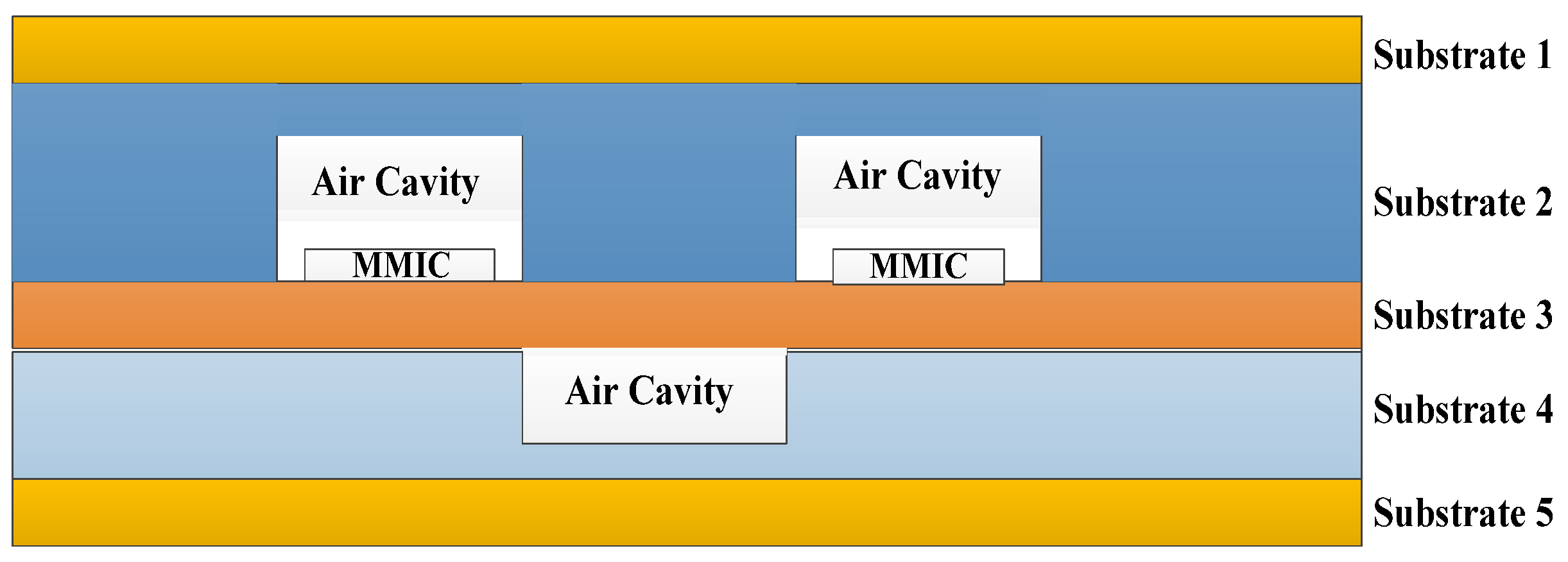
The composite laminate with a permittivity of 3.0 and a dielectric loss tangent of 0.0011 is used as the substrate. It shows the features of low dielectric loss and low gassing rate. Figure 2 shows the 5-layer SISL structure in our design, which consists of five PCB layers. The core RF circuits and MMICs are designed and assembled on the third substrate layer. The second and fourth substrate layers are hollowed out to form air cavities for the suspended strip line. The first and fifth layers are used as cover plates for the cavity. The metal layer at the bottom of the first substrate and the top of the fifth substrate, as well as the metalized holes surrounding the cavities that connect the first and fifth layers, form a shielding structure for the suspended stripline, which realizes the self-packaging structure, reduces the radiation loss, and shields the electromagnetic wave effectively.
3. Circuit Design
3.1. Layout Design
The proposed Ka-band two-channel two-beam receiver module based on SISL works in 28~30 GHz. It contains five substrate layers named sub1~sub5, as illustrated in Figure 3. Sub3 is the core RF layer where MMICs, including the LNA, two-channel multi-functional chips with amplitude and phase control, and transition circuits are integrated.
In the selection of dielectric thickness, the thinner the dielectric thickness, the smaller the loss, and it can effectively suppress the higher order modes generation, making it more suitable for applications in the Ka-band high-frequency range. Therefore, the thickness of dielectric substrate 3 as the core circuit layer should be as thin as possible. However, it is also important to ensure sufficient hardness to prevent deformation due to excessive thinness, which may affect the physical performance. Furthermore, the electromagnetic field of the SISL structure is mainly distributed in the air above and below the conductor instead of the lossy dielectric substrate, which makes the transmission property of SISL relatively less affected by the substrate property. Therefore, the thickness of dielectric substrate 3 is selected as 0.254 mm to ensure sufficient structural strength. Dielectric substrates 2 and 4 will be partially excavated to form the cavity layer for the SISL receiver component. Their thickness will directly determine the overall height of the shielding cavity. In the design of the Ka-band receiver component, to avoid cavity resonance and transmission of higher order modes and ensure that the component operates in single-mode transmission mode, the size of the shielding cavity should be small enough. However, the thickness of the dielectric substrate in the cavity layer should not be too thin as well, otherwise it may lead to insufficient hardness, uneven thickness, and other problems. In this design, a thickness of 0.508 mm is selected for sub 2 and sub 4.
3.2. Substrate Integrated Suspended Line Design
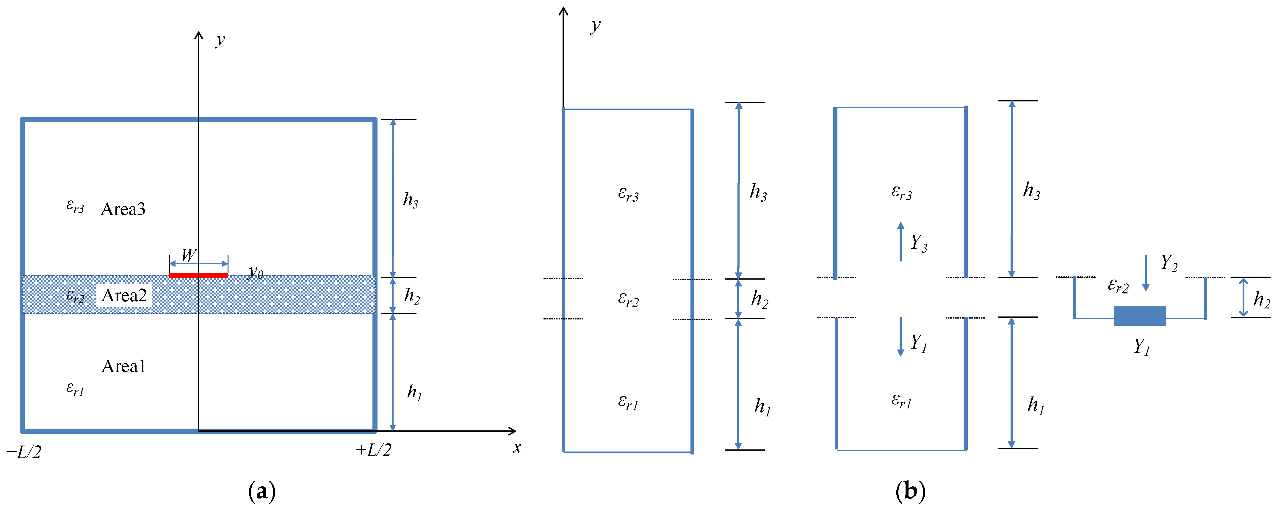
The SISL circuit is based on a suspended stripline, whose cross-section is illustrated in Figure 4a. The area 3 and 1 are air with permittivity of εr3 = εr1. The area 2 is the dielectric substrate. The transmission mode in SISL can be considered as quasi-TEM mode. The transmission characteristic of SISL can be derived from solving the distributed capacitance of the transmission line. The solution of the capacitance can be calculated using the variation method and Green function. The Green function can be derived from solving the effective circuit of the transmission line along the Y direction [20]. Here, we consider the SISL model in Figure 4a as a transmission line along Y direction, where the distribution of the electromagnetic wave is a standing wave. The effective circuit of the SISL along Y direction is shown in Figure 4b. It can be considered as a short-circuit line as the SISL is in a metal shielding cavity.
The input admittance of the short-circuit line can be written as
where , L is the width of the metal cavity, h1, and h3 are the height below and above the substrate of the SISL.
The input admittance of the loaded line can be written as
The overall admittance at y0 is
Then, the Green function at y = y0 can be written as
Based on the variation method, the stable variation of the capacity can be expressed as
where is the distribution of electric charge and w is the width of the SISL, as shown in Figure 4a.
The characteristic impedance of the SISL can be written as
where C′ is the capacity calculated when , C″ is the capacity calculated with the real permittivity of the substrate, and υ0 is the phase velocity in the SISL.
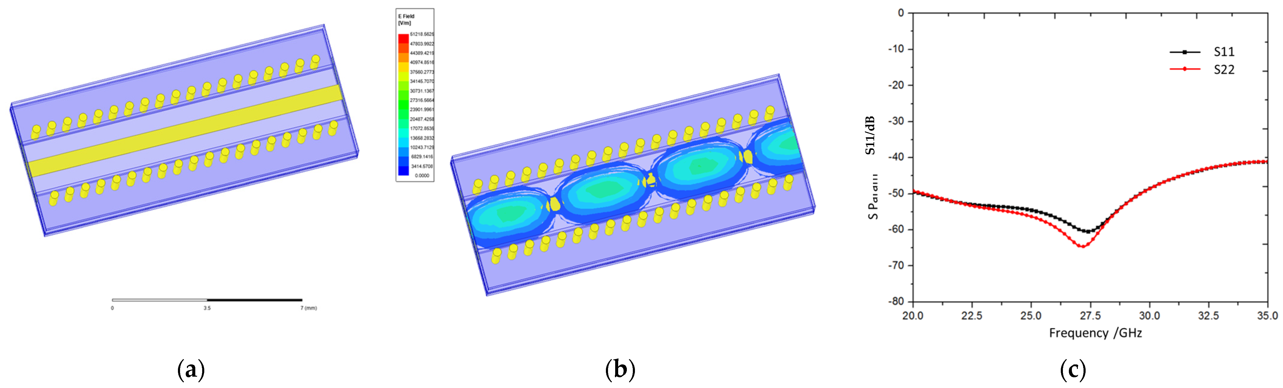
A SISL simulation model is built in HFSS. The simulation results show that the electric field is confined and transmitted in the air cavity surrounded by grounding via holes, as shown in Figure 5b. This validates the good inter-channel shielding performance. The return loss of the SISL is better than 40 dB over 20 GHz~35 GHz, as shown in Figure 5c.
In SISL circuits, the transmitted electromagnetic signals are confined by the metal vias on both sides of the transmission lines. On one hand, this avoids the resonance in the working frequency and improves the transmission performance. On the other hand, it effectively shields electromagnetic fields, reduces radiation, suppresses coupling and interference between adjacent transmission lines, and improves the density of wiring and packaging. According to the processing capabilities, the diameter of the via holes is selected as 0.3 mm.
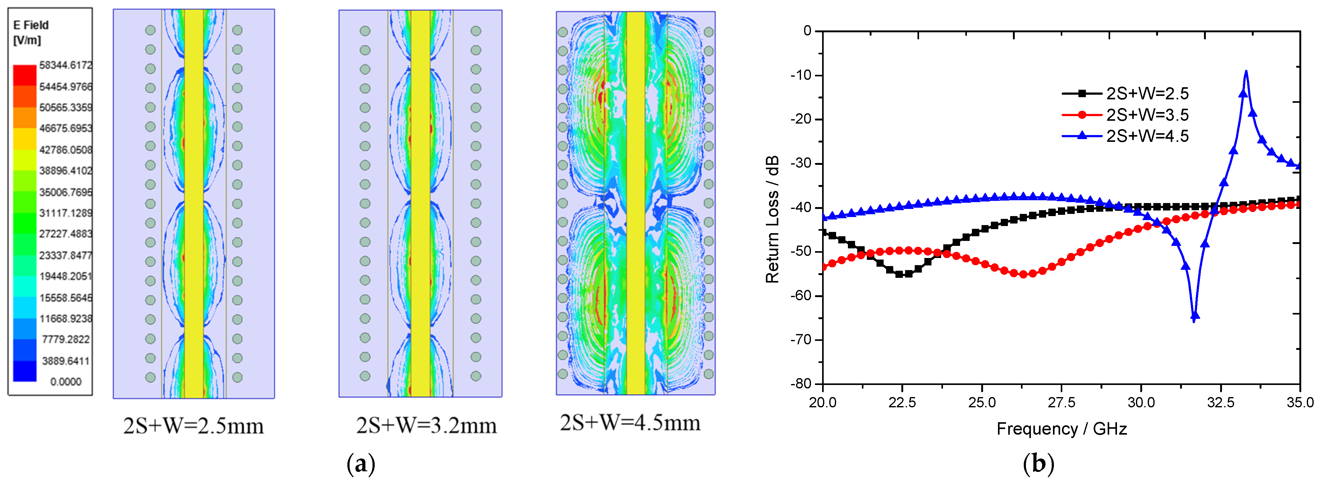
In practice, the spacing between two columns of shielding metal vias (2S + W) should not be too large, and it should satisfy the relationship below:
where the S is the space between the edge of the transmission line and via hole, W is the width of the transmission line, as shown in Figure 6.
When the distance between ground vias and transmission lines is too large, unwanted parasitic modes can be excited in the equivalent dielectric-filled ridge waveguide formed by two rows of metal vias and the ground plane, leading to unwanted resonance, which deteriorates the transmission performance of the circuit. The change of field distribution and return loss with the increase of the distance between ground vias and transmission lines is shown in Figure 7. When the 2S + W increases to 4.5 mm, more field is distributed in the substrate, and resonance can be observed in the frequency range of 20~35 GHz.
In practice, to enhance electromagnetic shielding, the via spacing should be as small as possible while meeting the fabrication capabilities. Especially in the Ka-band, where the wavelength of the signal is extremely short, the spacing of the via needs to be reduced accordingly. Typically, it is necessary to ensure that the spacing (center-to-center distance) between vias is greater than twice the diameter. In our design, the diameter of the via is 0.3 mm, and the spacing of the via is chosen to be 0.7 mm.
3.3. Coplanar Waveguide (CPW)–Stripline (SL)–SISL Transition Design
The RF signal is mainly transmitted along SISL in our design. In practice, the inner transmission line needs to transit to the coplanar waveguide for testing and interconnection with other modules. The transition structure consists of SISL, SL, and CPW [21]. The characteristic impedance of these three types of transmission lines is set as 50 Ohm. However, the width of the 50 Ohm-transmission line is different in different types of transmission lines, which makes it easy to generate reflection waves at transition points, leading to degradation of voltage standing wave ratio (VSWR). So the transition structure needs to be optimized at the transition point among SISL, SL, and CPW. As the reflection wave may couple to other substrate layers and cause resonance, the optimization of the transmission needs to consider the location of the SL layer as well. The model of the proposed CPW-SL-SISL transition and its simulation results are shown in Figure 8. The dimension of the transition is shown in Table 2.
The transition circuit exhibits good matching and transmission performance in the working bandwidth of 20~35 GHz. The return loss is better than 25 dB, as shown in Figure 8. A back-to-back transition model is also built and analyzed, as shown in Figure 9. Return losses of better than 27 dB are observed at two ports in the frequency range of 20~35 GHz, which shows good transmission performance.
3.4. Assembly Process
The packaging technique used in this design is the substrate stacking soldering process. The photos of the substrates 1~5 are shown in Figure 10a. Firstly, substrates 2, 3, and 4 are soldered together using a tin–silver–copper solder with a thickness of 40 μm and a melting point of approximately 217 °C. The active devices are also assembled in this process. The soldered substrates 2, 3, and 4 are shown in Figure 10b. Then, substrates 1 and 5 are soldered to the previous three layers using a tin–lead solder with a melting point of approximately 183 °C. Three positioning holes are designed to guarantee proper alignment between the substrates using positioning pins. It can be seen that the entire substrates are integrated properly, making it more convenient for interconnection with other circuits and ensuring good reliability, as shown in the X-ray photos in Figure 10c. Based on the substrate soldering technique, good inter-layer grounding characteristics are achieved, providing better RF shielding for the millimeter-wave frequency band.
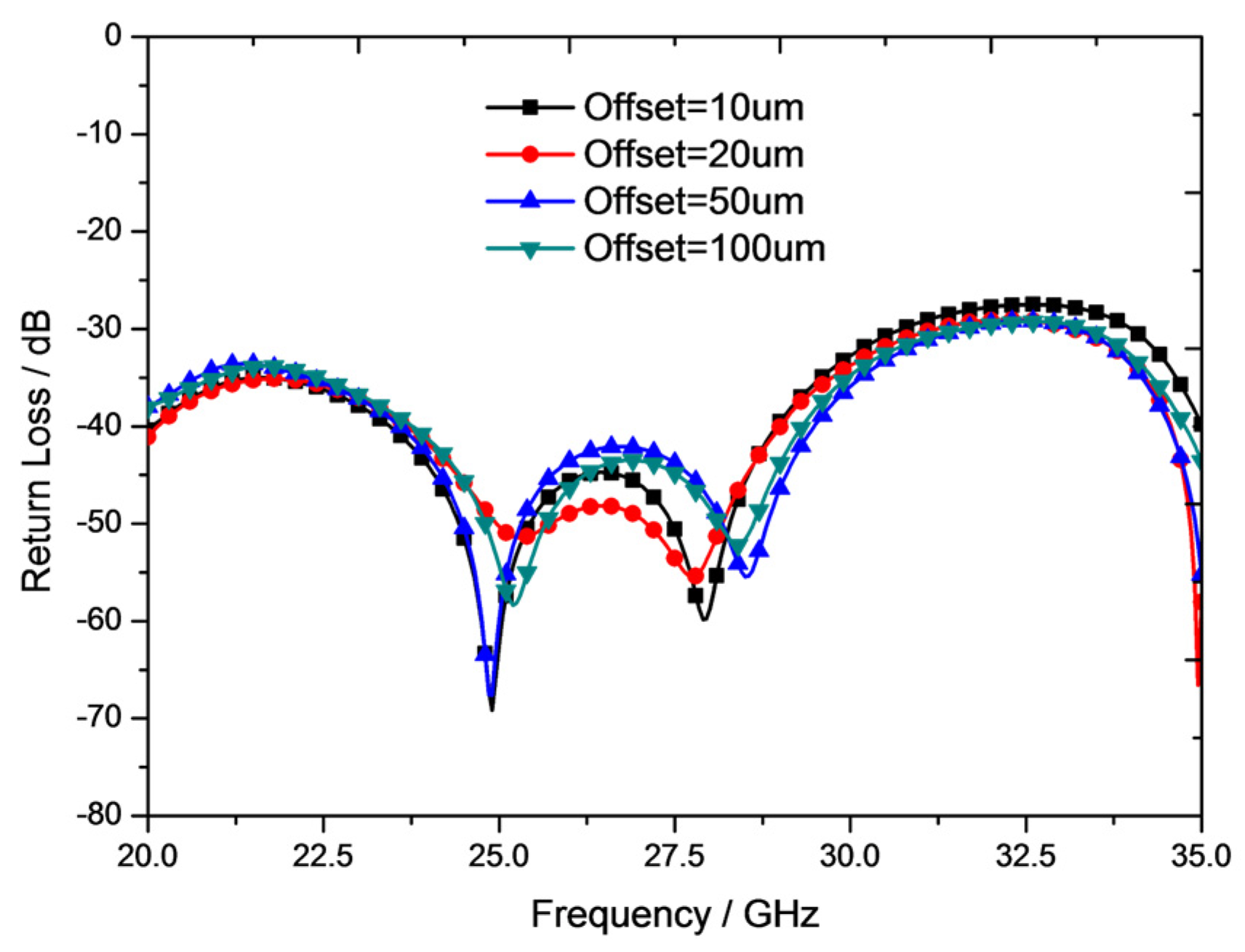
Wafer stacking is a crucial step in the implementation of SISL circuits, involving the vertical assembly and fixation of multiple substrate assemblies with integrated chips using appropriate methods. During substrate stacking, precise positioning and fixation of the substrates are required to ensure that the vertical interconnection points between layers are aligned accurately in three-dimensional space. However, when the five-layer dielectric substrates are assembled, there will inevitably be certain positional deviations between each layer, which makes it difficult to form effective vertical interconnection, leading to a deterioration of the RF performance. To address this issue, non-metallic positioning holes are machined at the same position on each layer of the dielectric substrate, and positioning is done using dowel pins before welding assembly. This can minimize the positional deviations between the layers. The typical value for alignment accuracy is 30 μm. The impact of misalignment in the positioning of the five-layer boards on RF performance is simulated, as shown in Figure 11. When deviations change from 10 μm to 100 μm, the return losses remain better than 27 dB, which shows a negligible effect on the RF performance.
The thickness of the PCB substrate may have certain deviations between different batches (typically within 10%). These thickness differences have a relatively minor impact on circuit designs in the low-frequency range. However, when the working frequency rises to the millimeter-wave frequency range where wavelengths are very short, the accumulation of these errors may lead to deterioration in the overall performance of the circuit. Here, an analysis of the impact of substrate thickness deviation on the RF performance of the circuit is conducted, as shown in Figure 12. The RF performance of the circuit is simulated under thickness deviations of 5%, 10%, and 20% at the main circuit layer with a nominal thickness of 0.254 mm. It can be observed that within a thickness deviation of 10%, the return loss is maintained better than 27 dB. Even under a thickness deviation of 20%, the return loss is still better than 20 dB.
To achieve the stacking and soldering of five-layer substrate layers, in the beginning, a large-area grounding is adopted in the layout design of the circuit board. However, During the circuit soldering process, it was found that insufficient pressure during soldering would lead to poor contact at the interconnection points, while excessive pressure would make the solder flow from the grounding position into other interconnected positions, resulting in short circuits. To address this problem, the laser scribing method was adopted to divide the grounding pads, which increases the distance between the grounding pad and other points. The area where the metal layer is removed after laser scribing can also serve as a solder resistor, which can prevent solder from flowing. In this way, moderate pressure can be applied to the substrate during soldering, and the solder at the grounding pad will not flow into other interconnected points, ensuring both the reliability of the interconnection and avoiding short circuits. In the proposed design, optimization of the soldering grounds pattern is carried out. The large ground pad are only used in the sensitive grounding areas, while in other parts, a grid design is implemented to meet process requirements, as shown in Figure 13. The recommended parameters are listed in Table 3 according to the fabrication capability.
4. Receiver Module Measurement
The assembled two-channel two-beam receiver module is shown in Figure 14a. As it is self-packaged, no external metal cavity is needed. The dimension of the module is 55 mm × 55 mm × 1.8 mm. The setup to measure the receiver module is shown in Figure 14b. The power supply provides +5 V DC voltage to drive the active components in the module. A serial instruction controller controlled by the computer sends instructions to control the attenuation and phase shifting in each channel. The gain and the manipulation of the attenuation and phase shift are measured with an S-parameter testing using a vector network analyzer (VNA). The NF is measured by the signal analyzer. The root mean square resolution of amplitude and phase control is acquired via post-processing of attenuation and phase shifting data.
In the S-parameter test, firstly, the VNA is calibrated in the frequency range of 28~30 GHz to calibrate the error and losses in the test equipment and RF cable. Then, the receiver module is connected to the test setup, as shown in Figure 14b. The single-channel ground-state gain, where the digital control attenuator is set as 0 dB, is shown in Figure 15a. The in-band receiving gain exceeds 28 dB in 28~30 GHz range. The control of attenuation and phase-shifting is shown in Figure 15c,d. The attenuation can be adjusted from 0.5 dB to 23.5 dB with an increment of 0.5 dB. The phase shift of the module can be changed over 360° with a step of 5.625°. The RMS resolution of attenuation and phase shifting are 1 dB and 4°, respectively.
In the NF testing, a signal analyzer is used in combination with a noise source probe to measure the NF based on the Y-factor method. Firstly, the noise source probe is directly connected to the signal analyzer to calibrate the equipment. Then, the input port of the receiver is connected to the noise source probe, and the output port is connected to the signal analyzer for NF testing. The ground-state NF is less than 2.6 dB in 28~30 GHz range, as shown in Figure 15b. The measured NF accords with the link budget analysis in Table 1. A lower NF of 1.4 dB at the frequency of 28.25 GHz and a relatively large in-band NF fluctuation are observed in Figure 15b. Two reasons can lead to this result. One is that the LNA chip used in this design is a commercial chip that is not optimized in the working frequency. In general, it has a lower NF in the lower frequency. The other is that the assembly error of the connector will accumulate to the assembly error of the multi-layer structure, which will influence the impedance matching at the input port, leading to a relatively large insertion loss at a higher frequency. The large insertion loss of the input connector will directly deteriorate the NF of the module leading to a relatively large NF fluctuation.
A performance comparison is made in Table 4. It can be observed from the table that the proposed module shows the best NF and a moderate receiving gain. The size of the proposed receiver is relatively large. This is mainly because only five layers of substrates are used in the design, and vertical dimensions are not well used. If more layers of substrates are used, more layers of SISL can be formed, and the chips can be packaged in a 3-D way. Another thing that needs to be pointed out is that the proposed design is implemented in PCB circuits, which shows great advantages in cost compared with the module implemented via LTCC or semiconductor technology. The results validate the feasibility of the proposed design for the demand for large-scale active phased-array antenna.
5. Conclusions
We propose a novel two-channel two-beam receiver module for the Ka-band application based on the SISL structure. The passive circuits are integrated as a whole through the SISL structure. A multi-layer spatial distribution of RF circuits, low-frequency circuits, and multi-layer components is formed through a multi-layer microwave substrate, creating a multi-layer assembled three-dimensional structure and eliminating the discontinuity introduced by circuit interconnections. At the same time, multiple independent cavities are formed, where active devices can be embedded to shield microwave radiation signals, leading to a significant reduction of interference between various microwave signals, self-packaging, and excellent electromagnetic compatibility. Through process improvement, the soldering points in the circuit design have been enhanced by changing the large-area grounding to a grid grounding, assuring the soldering quality and reliability of the circuit. This design is suitable for high-frequency band, low-cost, highly integrated channel design, and has good potential for widespread application and promotion.
Author Contributions
Conceptualization, H.X. and K.M.; methodology, H.X., S.L. and K.M.; validation, H.X., S.L. and G.L.; formal analysis, H.X., S.L. and G.L.; investigation, H.X., S.L., G.L. and Y.W.; data curation, H.X. and S.L.; writing—original draft preparation, H.X., S.L. and G.L.; writing—review and editing, H.X., K.M. and Y.W.; visualization, S.L. and G.L.; supervision, K.M. All authors have read and agreed to the published version of the manuscript.
Funding
This research was funded by the National Natural Science Foundation of China under Grant 62341409.
Data Availability Statement
The data that support the findings of this study are available from the corresponding authors upon reasonable request.
Acknowledgments
The authors would like to thank colleagues at Tianjin University and CAST (Xi’an) for their kind help and useful discussion during the research.
Conflicts of Interest
The authors declare no conflicts of interest.
References
- Yu, L.; Lei, L.; Zhang, K.; Wang, J.; Zhang, Q.; Li, Y.; Mao, L. Research progress and development trends on lowe-arth-orbit spaceborne multi-beam phased array antennas. Space Electron. Technol. 2022, 19, 1–11. [Google Scholar]
- Wang, J.; Liu, Y. Application and Prospect of Phased Array Antenna in Satellite Communications. Radio Eng. 2019, 49, 1076–1084. [Google Scholar]
- Ren, J.Q.; Zhou, H.G.; Zhou, N.; Liu, Q. Application of Phased Array Antenna and Fixed Multibeam Antenna in Communications Satellite Systems. Space Int. 2015, 443, 55–60. [Google Scholar]
- Wang, C.; Wang, Y.; Lian, P.; Xue, S.; Xu, Q.; Shi, Y.; Jia, Y.; Du, B.; Liu, J.; Tang, B. Space Phased Array Antenna Developments: A Perspective on Structural Design. IEEE Aerosp. Electron. Syst. Mag. 2020, 35, 44–63. [Google Scholar] [CrossRef]
- He, G.; Gao, X.; Sun, L.; Zhang, R. A Review of Multibeam Phased Array Antennas as LEO Satellite Constellation Ground Station. IEEE Access 2021, 9, 147142–147154. [Google Scholar] [CrossRef]
- Zeng, Q.; Chen, Z.; He, M.; Wang, S.; Liu, X.; Xu, H. Design of a Ka-Band Heterogeneous Integrated T/R Module of Phased Array Antenna. Electronics 2024, 13, 204. [Google Scholar] [CrossRef]
- Li, Z.; Sun, H.; Wu, H.; Zhang, S. An Ultra-Wideband Compact TR Module Based on 3-D Packaging. Electronics 2021, 10, 1435. [Google Scholar] [CrossRef]
- Ma, K.; Chan, K.T. Quasi-Planar Circuits with Air Cavities. PCT Patent WO/2007/149046, 27 December 2007. Available online: https://patentscope.wipo.int/search/en/detail.jsf?docId=WO2007149046 (accessed on 15 April 2024).
- Ma, K.; Yan, N.; Wang, Y. Recent Progress in SISL Circuits and Systems: Review of Passive and Active Circuits Demonstrating SISL’s Low Loss and Self-Packaging and Showcasing the Merits of Metallic, Shielded, Suspended Lines. IEEE Microw. Mag. 2021, 22, 49–71. [Google Scholar] [CrossRef]
- Cai, J.; Dong, Y. Miniaturized, Low Loss Bandpass Filters Based on SISL Technology with Improved Stopband Rejection. In Proceedings of the 2023 IEEE MTT-S International Wireless Symposium (IWS), Qingdao, China, 16–19 May 2023; pp. 1–3. [Google Scholar]
- Kenney, R.H.; Walker, C.J.; Sigmarsson, H.H.; McDaniel, J.W. A Varactor-Based Tunable Combline Bandpass Filter Using Suspended Integrated Stripline (SISL). IEEE J. Miniaturization Air Space Syst. 2021, 2, 112–116. [Google Scholar] [CrossRef]
- Ma, L.; Wu, Y.; He, C.; Wang, W.; Liu, Y. A wideband filter-integrated coupler using substrate integrated suspended line (SISL) technology with patterned substrate. In Proceedings of the 2018 International Applied Computational Electromagnetics Society Symposium—China (ACES), Beijing, China, 29 July–1 August 2018; pp. 1–2. [Google Scholar]
- Xiao, J.; Ren, X.; Guo, K. High selective dual-band filtering power divider using self-packaged SISL. Electron. Lett. 2020, 56, 937–940. [Google Scholar] [CrossRef]
- Zhang, Y.; Zhou, H.; Feng, L.; Zhang, X.; Zhang, X.; Shi, W. Compact wideband filtering Balun Based on SISL Technology. Int. J. Microw. Wirel. Technol. 2023, 15, 1656–1661. [Google Scholar] [CrossRef]
- Zheng, Z.; Tan, X.; Li, D.; Li, M.; Chen, Q. Compact Dual-Band SISL Filtering Antennas with High Selectivity Based on Dual Gap-Coupled Patches. IEEE Trans. Antennas Propag. 2023, 71, 7892–7902. [Google Scholar] [CrossRef]
- Luo, T.; Yang, W.; Xue, Q.; Che, W. A High-Efficiency SISL-Based Slot Antenna Array for Wireless Power Transmission Application. IEEE Antennas Wirel. Propag. Lett. 2023, 22, 674–678. [Google Scholar] [CrossRef]
- Aakash; Rai, A.K.; Vishwakarma, R.; Bhattacharya, S.; Srivastava, K.V. Dual-Circularly Polarized Antenna Array for Automotive Radar at 77 GHz based on SISL Topology. In Proceedings of the 2023 IEEE Microwaves, Antennas, and Propagation Conference (MAPCON), Ahmedabad, India, 10–14 December 2023; pp. 1–4. [Google Scholar]
- Hong, X.; Ma, K.; Wang, Y. An Ultra-Low Noise LNA Based on SISL Platform for Ka-band Satellite Communication. IEEE Microw. Compon. Lett. 2024, 34, 199–202. [Google Scholar] [CrossRef]
- Liang, W.; Ma, K.; Chen, X.; Wang, Y. FR4-Based Low Phase Noise SISL VCO Using Tunable Weakly Coupled Resonators. IEEE Microw. Compon. Lett. 2022, 32, 72–75. [Google Scholar] [CrossRef]
- Wang, J.; Wu, W. Millimeter Wave Integrated Circuits Design and Application; Xidian University Press: Xi’an, China, 1985. [Google Scholar]
- Wang, J.; Li, D.; Shi, L.; Zhang, L.; Chen, X.; Chen, Q. A DC-40 GHz Substrate Integrated Suspended Line (SISL) to GCPW Transition. In Proceedings of the 2023 International Conference on Microwave and Millimeter Wave Technology (ICMMT), Qingdao, China, 14–17 May 2023; pp. 1–3. [Google Scholar]
- Yang, D.; Zhao, Y. A Ka Band Four-Channel Short Brick-Type 3D Integrated T/R Microsystem with Silicon-Based MEMS Technology. IC Des. 2023, 48, 506–511. [Google Scholar]
- Yu, F.; Guo, X.; Ma, S.; Wang, C.; Feng, G.; Wang, Z. Design and Fabrication of a TR Microsystem in Ka-Band with Si-Based 3D Heterogeneous Integration. In Proceedings of the IEEE Transactions on Components, Packaging and Manufacturing Technology, Aurora, CO, USA, 28–31 May 2024. [Google Scholar]
Figure 1.
Schematic of two-channel two-beam receiver. Paths in green and red form beam 1 (B1) and beam 2 (B2) respectively. CH1: channel 1, CH2: channel 2, LNA: low noise amplifier.
Figure 1.
Schematic of two-channel two-beam receiver. Paths in green and red form beam 1 (B1) and beam 2 (B2) respectively. CH1: channel 1, CH2: channel 2, LNA: low noise amplifier.

Figure 2.
Cross-sectional view of the 5-layer SISL structure.

Figure 3.
Layer structure of SISL. (a) 3-D view, (b) details of the core circuit (substrate 3).

Figure 4.
Schematic of SISL. (a) Cross-section, (b) equivalent circuit.

Figure 5.
Simulation of SISL. (a) Simulation model, (b) electric field distribution, (c) simulation results.
Figure 5.
Simulation of SISL. (a) Simulation model, (b) electric field distribution, (c) simulation results.

Figure 6.
Cross section of the SISL.

Figure 7.
The influence of the change of 2S + W on the RF performance of SISL. (a) Field distribution, (b) return loss.
Figure 7.
The influence of the change of 2S + W on the RF performance of SISL. (a) Field distribution, (b) return loss.

Figure 8.
Coplanar waveguide–Stripline–Suspended stripline transition simulation. (a) Simulation model, (b) simulation results.
Figure 8.
Coplanar waveguide–Stripline–Suspended stripline transition simulation. (a) Simulation model, (b) simulation results.

Figure 9.
Back-to-back CPW-SL-SISL transition simulation. (a) Simulation model, (b) simulation result.
Figure 9.
Back-to-back CPW-SL-SISL transition simulation. (a) Simulation model, (b) simulation result.

Figure 10.
Photos of the proposed SISL. (a) Separated substrate layers, (b) soldered substrate 2, 3, 4, (c) X-ray photo of the soldered substrate 2, 3, 4.
Figure 10.
Photos of the proposed SISL. (a) Separated substrate layers, (b) soldered substrate 2, 3, 4, (c) X-ray photo of the soldered substrate 2, 3, 4.

Figure 11.
Influence of substrate position deviation on return loss of circuit.

Figure 12.
Influence of substrate thickness deviation on return loss of circuit.

Figure 13.
Grounds pattern in grid design. A is the gap between the edge of the substrate and the metal ground. B is the gap between two metal ground strips in the y direction. C is the width of the metal ground strip. D is the gap between two metal ground strips in the x direction.
Figure 13.
Grounds pattern in grid design. A is the gap between the edge of the substrate and the metal ground. B is the gap between two metal ground strips in the y direction. C is the width of the metal ground strip. D is the gap between two metal ground strips in the x direction.

Figure 14.
(a) The photo of the assembled receiver module. (b) Measurement setup.

Figure 15.
Measurement results of the proposed receiver module (a) Gain, (b) NF, (c) Attenuation. Two 8 dB attenuators in the digital control attenuator chip are labeled as 8 dB (1) and 8 dB (2) respectively. (d) Phase shifting.
Figure 15.
Measurement results of the proposed receiver module (a) Gain, (b) NF, (c) Attenuation. Two 8 dB attenuators in the digital control attenuator chip are labeled as 8 dB (1) and 8 dB (2) respectively. (d) Phase shifting.


Table 1.
Link budget analysis of receiver module.
| Components | Gain of Components (dB) | Noise Figure of Components (dB) | Link Gain (dB) | Link Noise Figure (dB) |
|---|---|---|---|---|
| Connector Soldering | −0.8 | 0.8 | −0.8 | 0.800 |
| LNA1 | 27 | 1.7 | 26.2 | 2.500 |
| Attenuator | −2 | 2 | 24.2 | 2.503 |
| LNA2 | 27 | 1.7 | 51.2 | 2.508 |
| 6-bit Phase Shifter and Attenuator Chip | −17 | 17 | 34.2 | 2.509 |
| 2:1 Combiner | −4 | 4 | 30.2 | 2.510 |
| Connector Soldering | −0.8 | 0.8 | 29.4 | 2.511 |
Table 2.
The dimension of the proposed CPW-SL-SISL transition.
| Parameter | Value (mm) |
|---|---|
| w1 | 0.24 |
| w2 | 0.16 |
| w3 | 0.6 |
| w4 | 2 |
| gap | 0.10 |
| L | 0.9 |
Table 3.
Parameters of grid pattern.
| A | B | C | D | |
|---|---|---|---|---|
| Typical Value | ≥0.2 mm | ≥0.4 mm | ≥0.2 mm | ≥0.4 mm |
| Minimum Value | 0 mm | 0.25 mm | 0.15 mm | 0.3 mm |
Table 4.
Performance comparison of Ka band T/R module.
| Time | Module | Frequency (GHz) | Technique | Size (mm) | Gain (dB) | NF (dB) |
|---|---|---|---|---|---|---|
| 2023 [22] | 4-channels T/R module | 33~37 | Silicon-based MEMs, TSV, 3D integration | 18 × 19.5 × 3 | 35 | 4.6 |
| 2024 [6] | 4-channels T/R module | 22~26 | LTCC, BGA, multi-material heterogeneous integration | 10.8 × 10 × 3 | 26 | 4.4 |
| 2024 [23] | 4-channels T/R module | 33~35 | Silicon 3D heterogeneous-integration | 9.5 × 9.8 × 2 | 25.5 | 5.7 |
| this work | 2-channels 2-beams R module | 28~30 | PCB, SISL | 55 × 55 × 1.8 | 28.5 | 2.6 |
Disclaimer/Publisher’s Note: The statements, opinions and data contained in all publications are solely those of the individual author(s) and contributor(s) and not of MDPI and/or the editor(s). MDPI and/or the editor(s) disclaim responsibility for any injury to people or property resulting from any ideas, methods, instructions or products referred to in the content. |
© 2024 by the authors. Licensee MDPI, Basel, Switzerland. This article is an open access article distributed under the terms and conditions of the Creative Commons Attribution (CC BY) license (https://creativecommons.org/licenses/by/4.0/).
Share and Cite
MDPI and ACS Style
Xu, H.; Ma, K.; Li, S.; Liu, G.; Wang, Y. A Ka-Band Two-Channel Two-Beam Receiver Based on a Substrate-Integrated Suspended Line. Electronics 2024, 13, 1582. https://0-doi-org.brum.beds.ac.uk/10.3390/electronics13081582
AMA Style
Xu H, Ma K, Li S, Liu G, Wang Y. A Ka-Band Two-Channel Two-Beam Receiver Based on a Substrate-Integrated Suspended Line. Electronics. 2024; 13(8):1582. https://0-doi-org.brum.beds.ac.uk/10.3390/electronics13081582
Chicago/Turabian StyleXu, Hui, Kaixue Ma, Shuantao Li, Gaojian Liu, and Yongqiang Wang. 2024. "A Ka-Band Two-Channel Two-Beam Receiver Based on a Substrate-Integrated Suspended Line" Electronics 13, no. 8: 1582. https://0-doi-org.brum.beds.ac.uk/10.3390/electronics13081582
Note that from the first issue of 2016, this journal uses article numbers instead of page numbers. See further details here.