
A Model Predictive Control Scheme with Minimum Common-Mode Voltage for PMSM Drive System Fed by VSI

1
Chongqing University-University of Cincinnati Joint Co-op Institute, Chongqing University, Chongqing 400044, China
2
School of Electrical Engineering, Chongqing University, Chongqing 400044, China
*
Author to whom correspondence should be addressed.
Machines 2024, 12(5), 292; https://0-doi-org.brum.beds.ac.uk/10.3390/machines12050292
Submission received: 21 February 2024
/
Revised: 22 April 2024
/
Accepted: 23 April 2024
/
Published: 26 April 2024
(This article belongs to the Topic Advanced Energy and Propulsion Technology for Electric and Intelligent Transportation)
Abstract
:Common-mode voltage (CMV) brings shaft voltage and shaft current, and corrodes the bearings of the permanent-magnet synchronous machine (PMSM), which affects the reliability of the whole PMSM drive system. Since the CMV applied by the zero voltage vectors (ZVVs) is three times that applied by the active voltage vectors (AVVs), a modulation scheme achieving minimum CMV without ZVV is proposed and introduced into the model predictive control structure for the PMSM drive system. Firstly, the whole modulation range is divided into three regions, including the low voltage modulation region (LVMR), high voltage modulation region (HVMR), and over-voltage modulation region (OVMR). Meanwhile, the regional boundary expression is derived. Then, the active zero-state pulse width modulation (AZSPWM) is adopted in LVMR. To improve the steady-state performance, near-state pulse width modulation (NSPWM) without opposite ZVVs is applied to the HVMR. Furthermore, when the reference voltage vector (VV) is located in OVMR, an optimal scheme is proposed to improve the dynamic response. Under the premise of no ZVV existing in the whole modulation region, simulation and experimental results show that the proposed hybrid modulation method can improve the steady-state and dynamic performance of the PMSM drive system.
1. Introduction
Due to their simple structure and bidirectional current conversion, three-phase pulse width modulation (PWM) voltage source inverters (VSIs) are widely used in renewable energy [1], electrified vehicles [2], rail transit [3], and other industrial fields. Permanent-magnet synchronous machine (PMSM) is one of the crucial parts of electrified transportation and vehicle technology, which aims to reduce pollutants and preserve fossil fuels. However, for the PMSM drive system fed by VSIs, the common-mode voltage (CMV) is generated by the high-frequency PWM process, which will lead to the shaft voltage and shaft current of the PMSM, corrode the bearings of the PMSM, and affect the reliability of the whole PMSM drive system [4]. Meanwhile, the electromagnetic interference generated by CMV damages its control system and affects the regular operation of other electrical equipment [5]. Therefore, reducing CMV is necessary to improve the performance and reliability of the PMSM drive system [6].
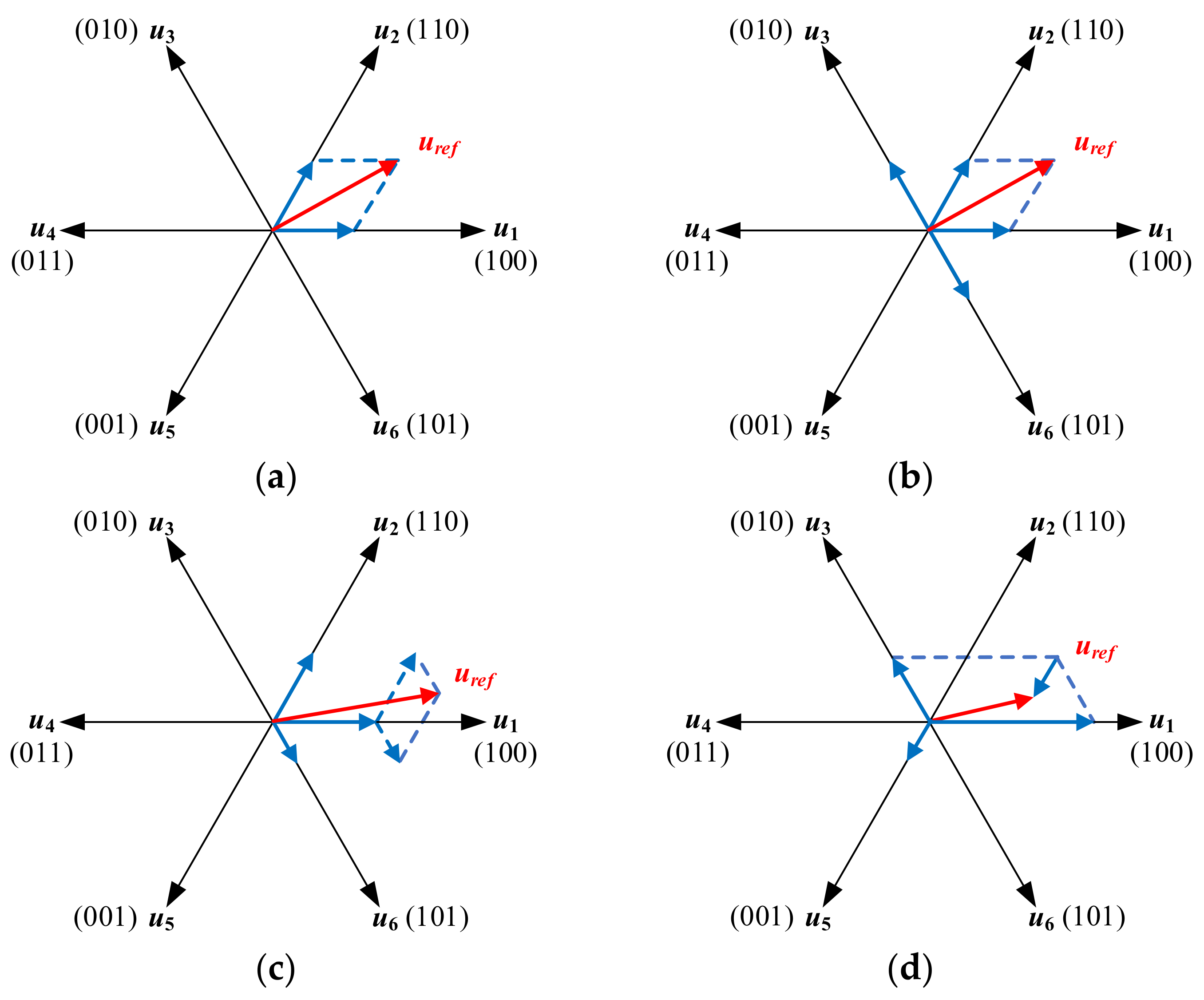
To avoid increasing hardware costs, improving the traditional SVPWM modulation scheme shown in Figure 1a has become a better choice [7]. Reference [8] indicates that the CMV in the zero voltage vector (ZVV) state is half of the DC-link voltage and is three times that in the active voltage vector (AVV) state, so changing the vector synthesis scheme by reducing or eliminating the dwell time of ZVV is an effective way to reduce CMV. The CMV suppression scheme is divided into SVPWM and carrier-based PWM schemes [9,10,11,12]. It mainly includes active zero-state PWM (AZSPWM), near-state PWM (NSPWM), and remote-state PWM (RSPWM). AZSPWM adopts two adjacent basic voltage vectors (VVs) and two opposite AVVs to replace the ZVV, as shown in Figure 1b; because it involves four VVs synthesizing the reference VV, the high-frequency CMV can be effectively reduced, but the resulting current harmonic is big. NSPWM adopts three adjacent AVVs to synthesize the reference VV, as shown in Figure 1c; it can reduce the high- and low-frequency CMV. Meanwhile, the switching is small. However, NSPWM is only suitable for the HVMR. If the reference is located in the LVMR, the ZVV will inevitably be introduced. At this time, the CMV magnitude is greater than that for AZSPWM applied in the LVMR. RSPWM1 and RSPWM2 adopt three even VVs and three odd VVs, in Figure 1d, respectively, to synthesize the reference VV. However, the maximum linear modulation region of these two is small. Furthermore, RSPWM3 can reduce high-frequency CMV by adopting mixed three even VVs and three odd VVs, achieving a wider modulation range. However, RSPWM3 still cannot cover the whole modulation region [13]. In [14,15], the impact of dead time on CMV is analyzed. To reduce the harmonic distortion of the current, an MPC scheme is proposed to use the six AVVs fully. However, the improvement effect is limited to situations with little dead time.
When the reference speed or load torque suddenly changes, the reference VV may be located in the overvoltage modulation region (OVMR), and there is an error between the reference VV and the synthesized VV [16]. Traditional SVPWM adopts the intersection point of the linear modulation boundary with reference VV as the synthesized VV [17]. However, it is not the optimal VV that has the least distance to the reference VV. Reference [18] shows that perpendicular feet from coordinates to the boundary line of the linear modulation is the optimal synthesized VV. However, the dwell time of the applied AVVs has not been derived.
Based on the advantages and disadvantages of the existing modulation scheme to suppress the CMV of VSI, this paper proposes an improved modulation scheme. The improved modulation scheme has separated the full modulation space into three different regions, including LVMR, HVMR, and OVMR, and corresponding optimal modulation schemes have been adopted for different regions. The AZSPWM and NSPWM are adopted for LVMR and HVMR, respectively. Additionally, when the reference VV is located in the OVMR, an improved overvoltage modulation PWM (IOMPWM) method with minimum voltage error is proposed. The proposed hybrid modulation scheme reduces CMV to the minimum, with improved dynamic performance and good steady-state performance.
This paper is organized as follows. Section 2 presents the deadbeat model predictive current control for the PMSM fed by VSI. Then, an improved hybrid modulation scheme is proposed in Section 3. Consequently, the effectiveness and superiority of the proposed scheme are validated by the simulation and experiment results in Section 4 and Section 5. Finally, the conclusion is drawn in Section 6.
2. Topology and Deadbeat Model Predictive Current Control
2.1. Topology of PMSM Fed by Voltage Source Inverter
Figure 2 shows the topology of the PMSM drive system fed by VSI, where Udc represents DC-link voltage, Cdc is the DC-link filter capacitor, S1, S2, S3, S4, S5, and S6 represent the switching tube of the VSI bridge.
2.2. Math Model Predictive Current Control for the PMSM Fed by VSI
According to [19], in the synchronous rotating frame (d-q frame), the current state equations of the PMSM are shown as
where ud and uq represent the stator voltage in the d-q frame, id and iq represent the stator current in d-q frame, Ld and Lq are the stator inductance in d-q frame, Rs is the stator resistance, ωe is the synchronous angle frequency, ψf is the flux linkage.
The equations of torque and speed are shown as
where Te and Tf represent the electromagnetic torque and load torque, np is the pole pairs, J is the moment of inertia, and ωe is the speed of the PMSM, respectively. This paper focuses on the surface mount PMSM as the research object, and Ld is equal to Lq, so Equations (3) and (4) are rewritten as
The first-order Euler formula is applied to Equations (1) and (2), the difference equation of current is derived as
where Ts is the control and sampling period.
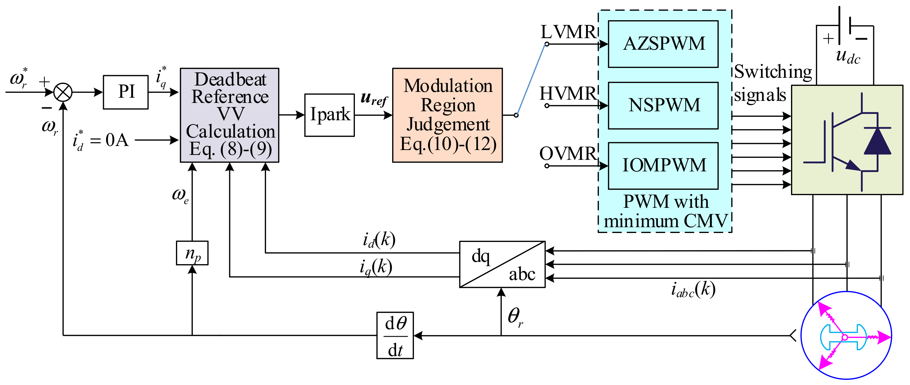
2.3. Deadbeat Model Predictive Current Control
The deadbeat model predictive current control (MPCC) scheme is adopted in this paper, the whole diagram is shown in Figure 3, where is the reference of iq, and is obtained by the speed PI controller. is the reference of id, and is set to zero.
According to the deadbeat condition, by replacing id(k + 1) and iq(k + 1) in Equations (6) and (7) with and , the reference of ud and uq can be obtained as
where and are the references of ud and uq.
Then, performing inverse Park transformation on and , the reference VV uref in the synchronous station frame can be obtained.
2.4. Conventional Vector Control Scheme
SVPWM is the conventional vector control strategy. Based on uref derived from MPCC, SVPWM can synthesize the uref using two adjacent VV and ZVV to generate the expected PWM signal to control the three-phase inverter. However, due to the impact of ZVV, the CMV peak value is Udc/2, and the six AVVs’ CMV peak value is Udc/6. The CMV peak value for eight basic VVs is summarized in Table 1.
3. Modulation Scheme with Minimum CMV
In Figure 4, the per-fundamental-cycle linearity regions (dark blue circular zones) and the per-PWM-cycle linearity regions (dark + light blue zones) of several modulations are illustrated. The standard SVPWM provides per-fundamental-cycle voltage linearity for 0 ≤ M ≤ 1. The per-carrier-cycle linearity range of these modulators covers the 3-phase inverter voltage hexagon shown in Figure 4a. The AZSPWM methods have the same voltage linearity characteristics as SVPWM. However, RSPWM methods exhibit different characteristics. Both RSPWM1 and RSPWM2 (Figure 4c) are linear inside either triangle T1 or T2, depending on which vector groups are selected. For the VVs u1, u3, u5, define T1 and VVs u2, u4, u6, define T2. The per-fundamental-cycle linearity range of either method is 0 ≤ M ≤ 0.57. RSPWM3 is linear inside the union of T1 and T2, which corresponds to a six-edged star (Figure 4d). The per-fundamental-cycle linearity of RSPWM3 is valid for 0 ≤ M ≤ 0.67 (corresponding to the largest circle inside the star). In contrast to RSPWM methods, NSPWM is linear at high M [0.57 ≤ M ≤ 1, Figure 4b]. In fact, these methods for some regions complement each other.
The modulation index M is the ratio between the magnitude of uref and half of the height of the whole region hexagon and is defined as
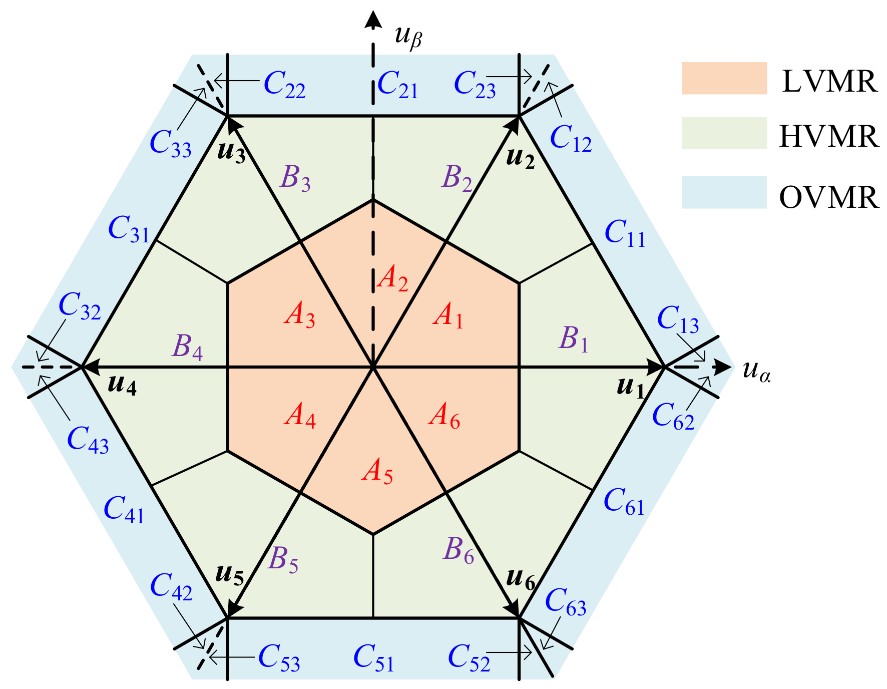
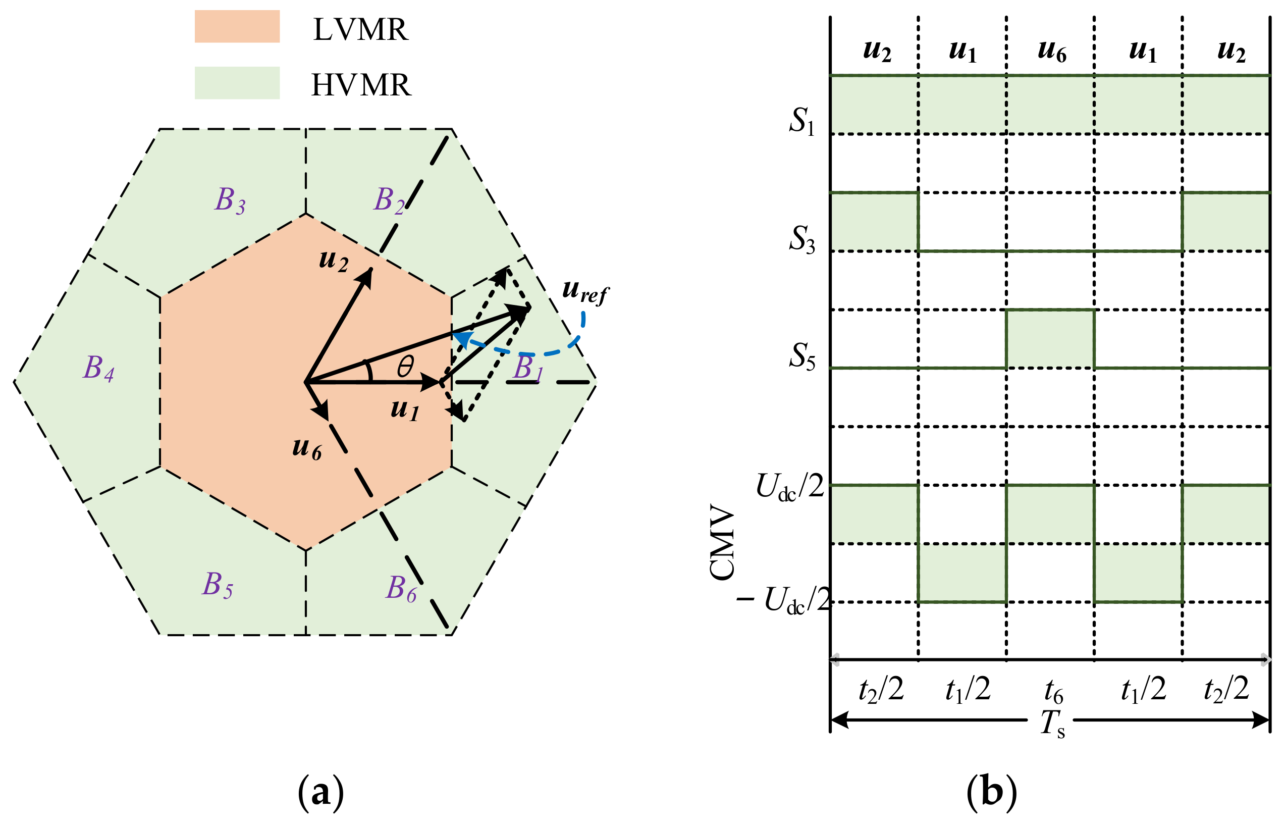
Considering the disadvantages and advantages of existing modulation schemes, in this paper, the whole space is separated into three regions, including LVMR, HVMR, and OVMR, which is adopted by AZSPWM, NSPWM, and improved overvoltage modulation PWM (IOMPWM), respectively. The diagram of the region division is shown in Figure 5. Compared to AZSPWM, NSPWM has the advantage of low switching loss and low current ripple. However, ZVV will be introduced if adopted in the LVMR, which causes a high CMV peak value. Therefore, NSPWM is adopted in HVMR, and AZSPWM is adopted in LVMR. Furthermore, an improved modulation scheme having the least error with reference voltage is proposed for OVMR. Overall, ZVV can be eliminated completely in the whole modulation range by the proposed hybrid modulation scheme.
3.1. Modulation Region Division
The division of three regions (LVMR, HVMR, and OVMR) is shown in Figure 5, and each region is further divided into several parts, where u1, u2, u3, u4, u5, and u6 represent the six basic AVVs. According to the linear modulation range and geometric analysis, the two specific boundary equations are derived as
In the equations above, , represent the coordinate in the synchronous static frame (α-β frame). The specific region division criterion of LVMR, HVMR, and OMVR are defined as
3.2. The Modulation Method of AZSPWM
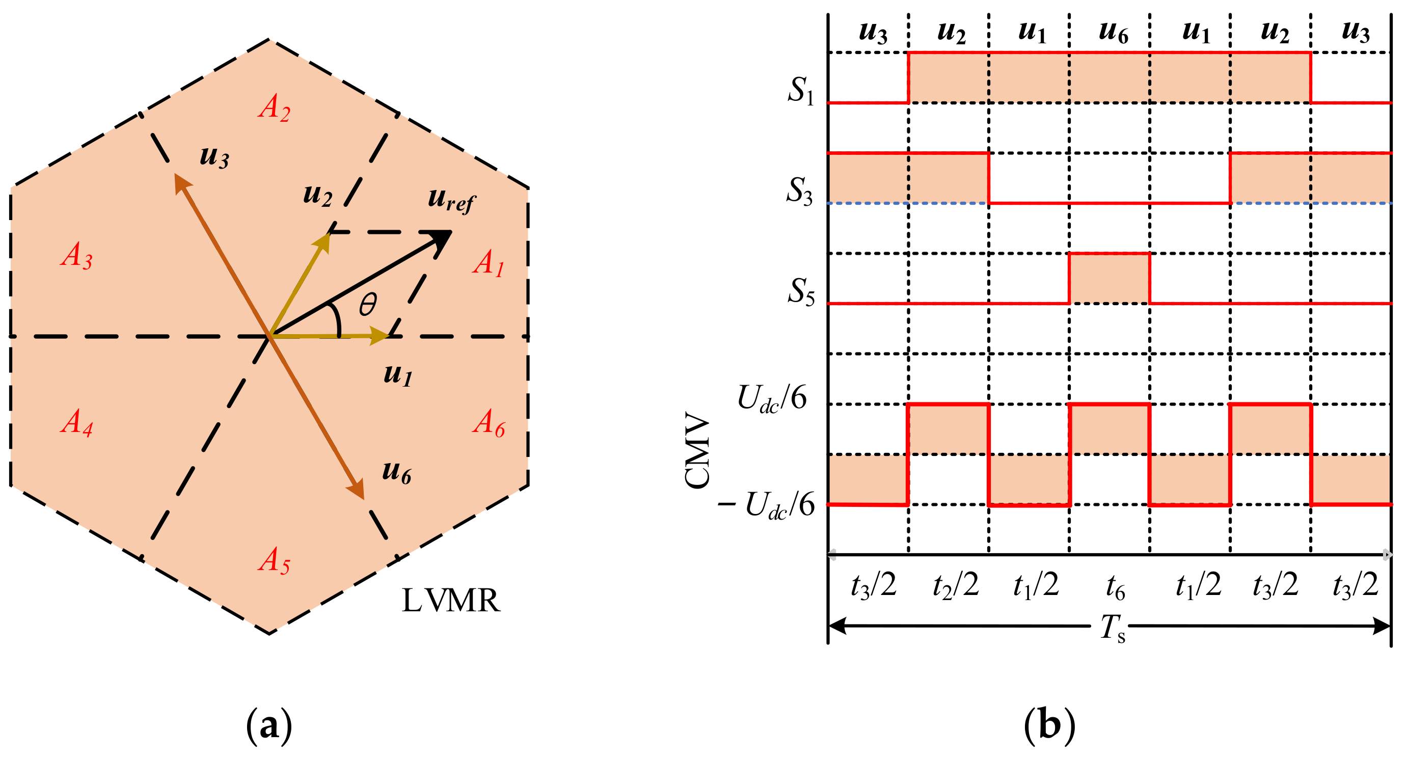
When uref is located in LVMR, the AZSPWM adopts two adjacent AVVs to synthesize uref and two AVVs with the same module length and opposite direction to replace ZVVs, supplementing the remaining time of the switching period. As shown in Figure 6a, the LVMR is divided into six zones (A1–A6).
Taking zone A1 as an example, AZSPWM adopts AVVs u1 and u2 to synthesize uref and adopts u3 and u6 in opposite directions to replace the ZVVs. The switching signals and CMV are shown in Figure 6b. Since the ZVV is eliminated, the CMV peak value of AZSPWM is Udc/6, which reduces the CMV to the minimum value. Furthermore, the dwell time of AVVs is derived as
where ti (i = 1,2,…,6) represents the dwell time of the corresponding ui, respectively. θ is the rotational angle of uref with the α axis.
When uref is located in other zones of LVMR, the applied VVs with dwell time are summarized in Table 2.
3.3. The Modulation Method of NSPWM
In the HVMR, NSPWM adopts a group of three neighbor AVVs to synthesize uref. These three AVVs are selected are closest to uref, and their two neighbors (to the right and left) are adopted. Since the ZVV is eliminated, the CMV peak value of NSPWM is Udc/6, which reduces the CMV to the minimum value. The adopted AVVs are changed every 60 degrees. Therefore, the diagram of region division and AVV synthesis are shown in Figure 7.
Define that uleft, umiddle, uright are adopted for uref. Taking zone B1 as an example, NSPWM adopts three adjacent AVVs u5, u1, u3 as uleft, umiddle, uright, respectively, to synthesize uref. Then, the complex variable volt-seconds balance equation and the PWM period constraint for NSPWM are given in generalized form for all regions.
In the above equation, tleft, tmiddle, tright are the dwell time of uleft, umiddle, uright, respectively. Furthermore, tleft, tmiddle, tright for all zones can be derived as follows:
In the above equation, i represents the zone number, which ranges from 1 to 6 [20].
AVVs with dwell time are summarized in Table 3 for uref in all zones of HVMR.
3.4. The Improved Overvoltage Modulation Scheme for OVMR
When the reference speed or load torque suddenly changes, uref may be located in the OVMR, and the amplitude of uref exceeds all synthesized VVs. In order to synthesize a reachable VV that has the least distance error from uref, an improved overvoltage modulation PWM (IOMPWM) is proposed. Taking sector I as an example, in Figure 8, the OVMR of sector I is divided into three zones, namely C11, C12, and C13. When uref (OM) is located in C11, OH is selected as the synthesized VV by traditional SVPWM. However, OG has less distance from uref than OH because MG is perpendicular to the boundary of the linear modulation. Therefore, OG is selected as the synthesized VV in this paper; it is synthesized by u1 and u2. The dwell time of u1 and u2 are derived as:
In Figure 8, when uref is located in C12, only u2 is applied in the whole control period. When uref is located in C13, only u1 is applied in the whole control period. The equation of the divided lines l12 and l13 is expressed as:
When uref is located in the OVMR of all sectors, the applied VV with dwell time is summarized in Table 4, where the number of zones is shown in Figure 8.
In this paper, the accuracy ratio of the conventional overvoltage modulation method is defined as ηSVPWM and can be derived as:
Similarly, the accuracy ratio of the proposed IOMPWM method is defined as ηIOMPWM and can be derived as:
According to the geographical relation, |HM| is larger than |GM|. Therefore ηIOMPWM is less than ηSVPWM, so compared with the conventional overvoltage modulation method, IOMPWM can obtain less error with the reference VV and generate higher iq.
The accuracy ratio of the conventional overvoltage modulation method and IOMPWM in all zones are summarized in Table 5.
4. Simulation Results
The simulation model of the proposed hybrid modulation with minimum CMV is established in the Matlab/Simulink environment, and the steady-state and dynamic performances are verified by the simulation results; the PMSM parameters are shown in Table 6.
4.1. Steady-State Performance of LVMR
When the PMSM operates at 200 rpm with the load of 5 N·m, uref is located in LVMR, the steady-state performance under AZSPWM is shown in Figure 9. It has great speed stability. Since the ZVV is eliminated, the amplitude of CMV is Udc/6. However, AZSPWM adopts two AVVs with opposite directions, which causes a serious current ripple, the THD is 15.17%, and the torque ripple is 0.2688 N·m.
The torque ripple is calculated in the equation below.
where N represents the total sample number, and Te_ripple represents the PMSM torque ripple.
Figure 10 shows the steady-state performance for NSPWM in LVMR; it is obvious that the ripple of the stator current and the torque ripple are lower than that of AZSPWM, the current THD is 13.08%, and the torque ripple is 0.1603 N·m. However, since the ZVV occurs in the modulation process, the amplitude of CMV is Udc/2, as shown in Figure 10b.
4.2. Steady-State Performance of HVMR
Next, the PMSM operates at 800 rpm with 5 N·m, uref is located in HVMR, and the steady-state performance for NSPWM is shown in Figure 12. The THD of the stator current is 12.63%, and the torque ripple is 0.2283 N·m also with good speed stability. In Figure 12b, the amplitude of CMV is Udc/6, which shows that NSPWM has no ZVV when uref is located in HVMR.
In order to reflect the superiority of NSPWM in HVMR, the performance of NSPWM is compared to AZSPWM, and the simulation results under AZSPWM are shown in Figure 13. The ripple of stator current and torque is greater than that under NSPWM, the THD is 13.92%, and the torque ripple is 0.2777 N·m. Therefore, on the basis of no ZVV, NSPWM is more suitable than AZSPWM for HVMR.
Similarly, the simulation results of SVPWM in HVMR are shown in Figure 14. Also, SVPWM has great speed stability, low current ripple, which is 6.05%, and low torque ripple, which is 0.1886 N·m. However, there is still ZVV in the HVMR, which causes the high CMV magnitude. The simulation under all methods are summarized in Table 7.
4.3. Improved Performance of OVMR
To prove the improved overvoltage modulation performance of the proposed method. The operation conditions are set to verify the effectiveness of IOMPWM compared with the traditional overvoltage modulation method.
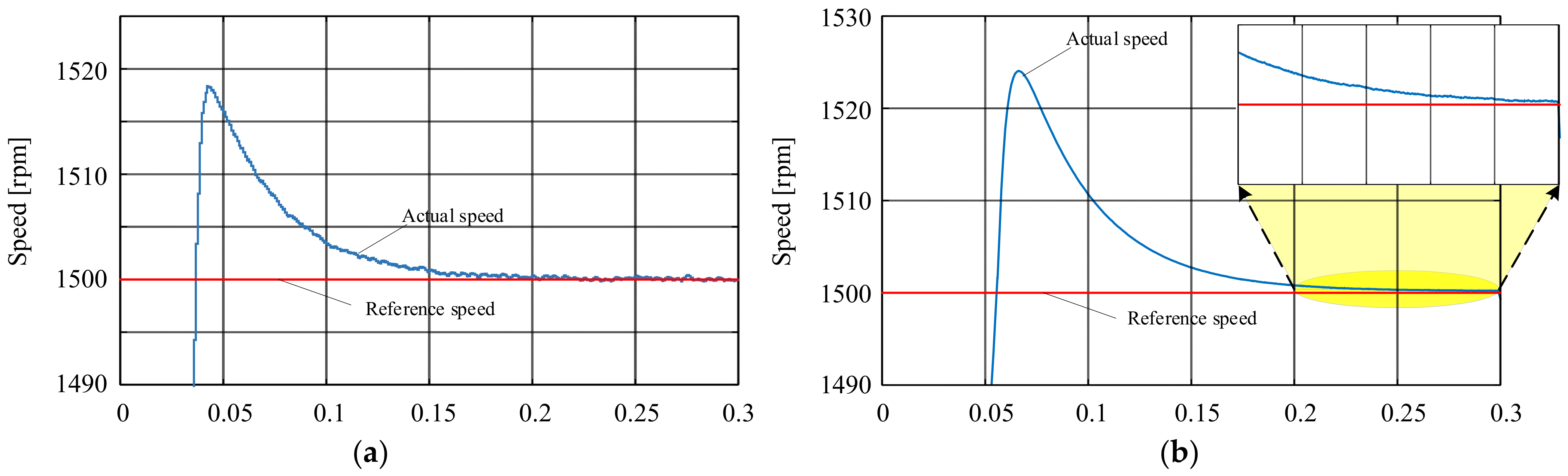
First, to test the dynamic improvement of IOMPWM, set the DC-link voltage source low to 210 volts, the PMSM control speed to 1500 rpm, and keep the speed PI controller and other conditions the same. It focuses on the start-up process and lets the reference VV located in the OVMR. In Figure 15 and Figure 16, the red lines represent the controlled speed reference, and the blue lines represent the PMSM speed. It shows that PMSM under IOMPWM reaches and remains steadily at 1500 rpm at 0.15 s. However, PMSM, under the conventional overvoltage modulation method, cannot even reach the controlled speed. It proves that IOMPWM can better utilize the DC-link voltage and generate bigger iq.
Second, to test the steady-state improvement of IOMPWM set the DC-link voltage to the original value and controlled speed to 1500 rpm. It focuses on the process after the speed overshoot. In Figure 16, the red lines represent the controlled speed reference value, and the blue lines represent the PMSM speed. The PMSM controlled by IOMPWM reaches and remains at the targeted speed at 0.2 s. However, the PMSM controlled by the conventional method has a bigger overshoot speed and also cannot reach the target speed even at 0.3 s.
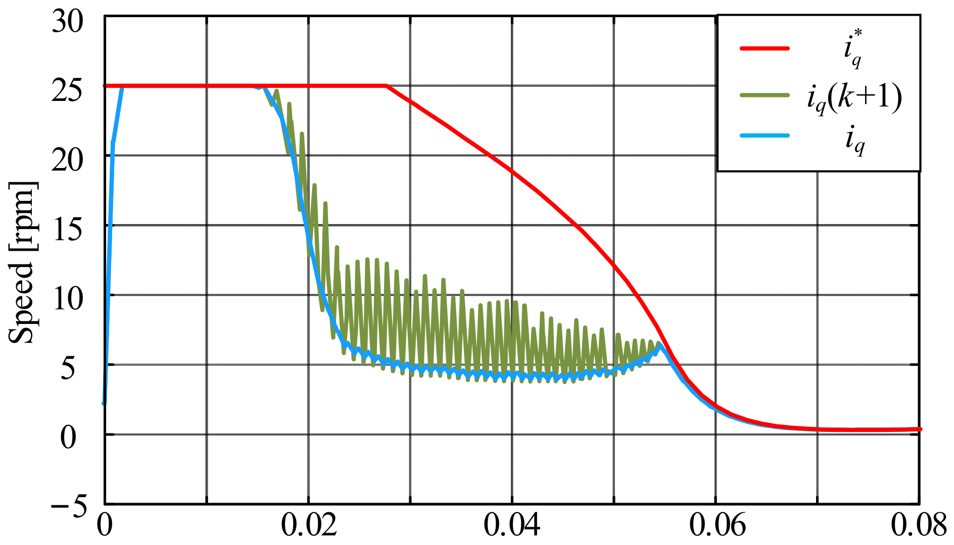
Furthermore, iq, , iq(k + 1) for traditional overvoltage modulation method are shown below. In Figure 17, represents the reference q-axis current generated by PI speed controller, iq(k + 1) represents the q-axis current generated by iq at kTs using IOMPWM. It shows that the actual q-axis current iq is always less than iq(k + 1) predicted by IOMPWM. Therefore, IOMPWM has better dynamic performance than SVPWM by providing a larger q-axis current.
5. Experimental Results
To demonstrate the effectiveness of the proposed modulation method, an experimental setup is established and shown in Figure 18. The VSI consists of an IGBT module FS400R07AE3 and a 400 μF/600 V film capacitor. The DC-link voltage 270 V is provided by the power supply PR300-4. The current sensors ACS724-10AB are used to measure the three-phase stator current. The sampling, control, and modulation algorithms are all executed in the DSP of TMS320F28335, and the carrier frequency and sampling frequency are both set to 10 kHz. The torque and speed are converted into analog signals with a refresh rate of 5 kHz through the DAC module. The parameters of the PMSM are presented in Table 4, and a magnetic powder brake with a rated torque of 5 N·m is used as the load of PMSM.
5.1. Steady-State Performance
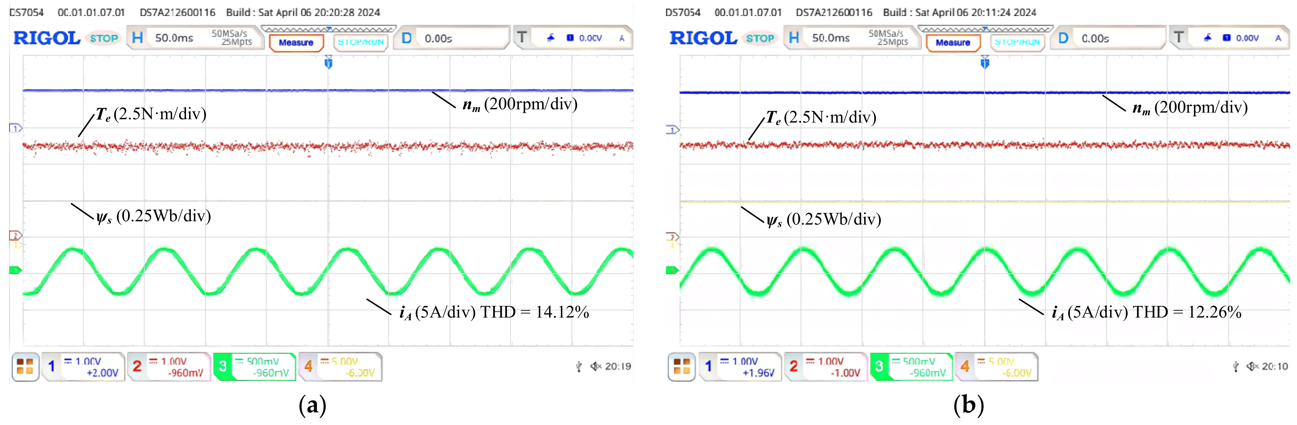
Experimental verification using the same operating conditions as simulation. For operational condition 200 rpm with the load of 5 N·m, uref is located in LVMR, which is controlled by AZSPWM in the proposed method. The steady experimental waveform for the proposed method and SVPWM are shown in Figure 19a,b, respectively. Both two modulation schemes get great speed and flux stability, also, the torque ripple can be derived from Equation (24), which is 0.0614 and 0.0428, respectively. Due to the four voltage vector synthesized strategy for AZSPWM, the THD of current for the proposed method is 14.12% and is greater than that for SVPWM, which is 12.26%. According to the definition of the CMV, the experimental waveforms of CMV under two modulation schemes are reconstructed based on the three-phase bridge arm voltage (uA, uB, and uC) and are shown in Figure 20. It can be seen that the amplitude of CMV for SVPWM is Udc/2, which is 3 times of the proposed method. The proposed method has greatly reduced the CMV peak value in LVMR.
For operational condition 800 rpm with the load of 5 N·m, uref is located in HVMR, which is controlled by NSPWM in the proposed method. Figure 21a,b shows the steady experimental waveform for the proposed method and SVPWM, respectively. A better steady-state performance can be obtained by the NSPWM, which is a three-voltage vector synthesized strategy. Both two modulation schemes get great speed and flux stability. Also, the torque ripple that can be derived from Equation (24) is 0.0564 and 0.0515, respectively. The THD of current for the proposed method is 11.13% and is bigger than that for SVPWM, which is 10.82%. In Figure 22, since no ZVV occurs in the modulation process in the NSPWM, the amplitude of CMV for NSPWM is Udc/6, which is the same as AZSPWM. The experimental results are consistent with simulation results, which show that NSPWM is the optimal modulation for HVMR. The steady-state experimental results are summarized in Table 8.
5.2. Dynamic Performance
To verify the dynamic control performance of the proposed method, the IOMPWM method, the start-up process, deceleration process, load torque increase process, and load torque decrease processes are set for the proposed method and SVPWM.
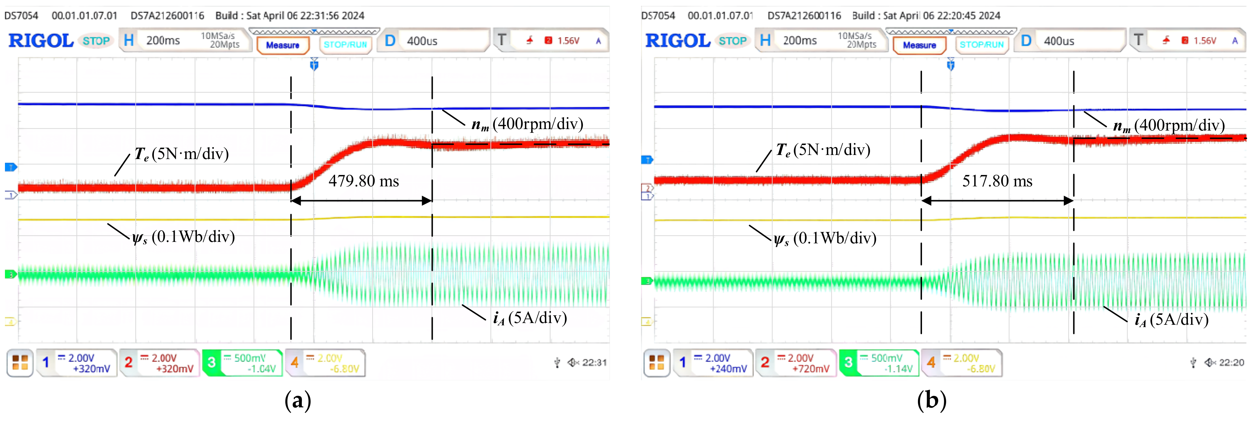
With the load of the load of 5 N·m, PMSM accelerates from 200 rpm to 800 rpm and decelerates from 800 rpm to 200 rpm; the dynamic experimental waveforms for the proposed method and SVPWM are shown in Figure 23 and Figure 24. When PMSM operates at the rated speed, it gives a sudden increase in load from 0 to 5 N·m and also a sudden decrease in load from 5 to 0 N·m; the dynamic experimental waveforms for the proposed method and SVPWM are shown in Figure 25 and Figure 26. Since the voltage vector with the minimum error between uref can be synthesized by the proposed IOMPWM in OVMR, the proposed method can generate a larger q-axis current and has a shorter dynamic response time. The total response time for load step and speed step experiments are summarized in Table 9.
6. Conclusions
In order to reduce the CMV of the PMSM drive system fed by VSI, this paper presents a hybrid modulation scheme without a zero voltage vector to achieve minimum CMV. Meanwhile, to maintain steady-state performance and improve dynamic performance, three regions are divided and matched to an optimal modulation scheme without a zero voltage vector. The feasibility and correctness are verified by the simulation and experimental results. The main conclusion could be summarized as follows.
- (1)
- AZSPWM is suitable for the whole modulation region. However, since two active voltage vectors with opposite directions are adopted, the current ripple and switching loss is greater than that under other modulation schemes.
- (2)
- The steady-state performance under NSPWM is better than that under AZSPWM. However, the zero voltage vector cannot be eliminated when the reference voltage vector is located in the low voltage modulation region, so it is suitable for the high voltage modulation region.
- (3)
- The proposed over-modulation scheme can synthesize the voltage vector with the minimum error between the reference voltage vector; therefore, an improved dynamic response can be obtained.
- (4)
- The switching loss of the proposed method has not been optimized. For HVMR, the NSPWM has redundancy on the sector division when the reference voltage is located near the sector boundary. It may be optimized by considering the power factor and adjusting the sector division criterion.
- (5)
- The current ripple of the proposed method is large due to adapting many basic vectors to synthesize the reference voltage. It can be optimized by adjusting the vector synthesizing sequence, but in this way, it may increase the switching number; therefore, it requires future study.
Author Contributions
Conceptualization and methodology, P.Q.; simulation, P.Q.; validation and experiment, P.Q. and J.X.; writing and supervision, P.Q. and F.M.; review and editing, P.Q.; funding acquisition, P.Q. All authors have read and agreed to the published version of the manuscript.
Funding
This research was funded by the Natural Science Foundation of Chongqing, China, grant number CSTB2022NSCQ-MSX0430.
Data Availability Statement
The data presented in this study are available upon request from the corresponding author.
Conflicts of Interest
The authors declare that there are no conflicts of interest regarding the publication of this paper.
References
- Jahan, S.; Biswas, S.P.; Haq, S.; Islam, M.R.; Mahmud, M.A.P.; Kouzani, A.Z. An Advanced Control Scheme for Voltage Source Inverter Based Grid-Tied PV Systems. IEEE Trans. Appl. Supercond. 2021, 31, 5401705. [Google Scholar] [CrossRef]
- Dong, Z.; Liu, C. Three-Dimension Space Vector Modulation for Three-Phase Series-End Winding Voltage-Source Inverters. IEEE Trans. Ind. Electron. 2024, 71, 82–92. [Google Scholar] [CrossRef]
- Miao, Y.; Liao, W.; Huang, S.; Liu, P.; Wu, X.; Song, P.; Li, G. DC-Link Current Minimization Scheme for IM Drive System Fed by Bidirectional DC Chopper-Based CSI. IEEE Trans. Transp. Electrif. 2023, 9, 2839–2850. [Google Scholar] [CrossRef]
- Yu, B.; Song, W.; Guo, Y. A Simplified and Generalized SVPWM Scheme for Two-Level Multiphase Inverters with Common-Mode Voltage Reduction. IEEE Trans. Ind. Electron. 2022, 69, 1378–1388. [Google Scholar] [CrossRef]
- Dabour, S.M.; Abdel-Wahab, S.M.; Rashad, E.M. Common-Mode Voltage Reduction Algorithm with Minimum Switching Losses for Three-Phase Inverters. In Proceedings of the 2019 21st International Middle East Power Systems Conference (MEPCON), Cairo, Egypt, 17–19 December 2019; Volume 9, pp. 1210–1215. [Google Scholar]
- Kan, S.; Ruan, X.; Huang, X.; Dang, H. Second Harmonic Current Reduction for Flying Capacitor Clamped Boost Three-Level Converter in Photovoltaic Grid-Connected Inverter. IEEE Trans. Power Electron. 2021, 36, 1669–1679. [Google Scholar] [CrossRef]
- Hota, A.; Agarwal, V. Novel Three-Phase H10 Inverter Topology with Zero or Constant Common-Mode Voltage for Three-Phase Induction Motor Drive Applications. IEEE Trans. Ind. Electron. 2022, 69, 7522–7525. [Google Scholar] [CrossRef]
- Guo, L.; Zhang, X.; Yang, S.; Xie, Z.; Cao, R. A Model Predictive Control-Based Common-Mode Voltage Suppression Strategy for Voltage-Source Inverter. IEEE Trans. Ind. Electron. 2016, 63, 6115–6125. [Google Scholar] [CrossRef]
- Xu, J.; Han, J.; Wang, Y.; Ali, M.; Tang, H. High-Frequency SiC Three-Phase VSIs with Common-Mode Voltage Reduction and Improved Performance Using Novel Tri-State PWM Method. IEEE Trans. Power Electron. 2019, 34, 1809–1822. [Google Scholar] [CrossRef]
- Tan, B.; Gu, Z.; Shen, K.; Ding, X. Third Harmonic Injection SPWM Method Based on Alternating Carrier Polarity to Suppress the Common Mode Voltage. IEEE Access 2019, 7, 9805–9816. [Google Scholar] [CrossRef]
- Zhang, Y.; Li, C.; Schutten, M.; De Leon, C.F.; Prabhakaran, S. Common-Mode EMI Comparison of NSPWM, DPWM1, and SVPWM Modulation Approaches. In Proceedings of the 2019 IEEE Energy Conversion Congress and Exposition (ECCE), Baltimore, MD, USA, 29 September–3 October 2019; pp. 6430–6437. [Google Scholar]
- Hava, A.M.; Ün, E. Performance Analysis of Reduced Common-Mode Voltage PWM Methods and Comparison with Standard PWM Methods for Three-Phase Voltage-Source Inverters. IEEE Trans. Power Electron. 2009, 24, 241–252. [Google Scholar] [CrossRef]
- Jun, E.-S.; Lim, D.H.; Heo, N.E. Development of PWM Module to Apply High-Performance RSPWM Control Method of Dual Inverter. In Proceedings of the 2023 IEEE Vehicle Power and Propulsion Conference (VPPC), Milan, Italy, 24–27 October 2023; pp. 1–6. [Google Scholar]
- Guo, L.; Jin, N.; Gan, C.; Xu, L.; Wang, Q. An Improved Model Predictive Control Strategy to Reduce Common-Mode Voltage for Two-Level Voltage Source Inverters Considering Dead-Time Effects. IEEE Trans. Ind. Electron. 2019, 66, 3561–3572. [Google Scholar] [CrossRef]
- Lai, Y.S.; Chen, P.S.; Lee, H.K.; Chou, J. Optimal common-mode Voltage reduction PWM technique for inverter control with consideration of the dead-time effects-part I: Basic development. IEEE Trans. Ind. Appl. 2004, 40, 1605–1612. [Google Scholar] [CrossRef]
- Sarajian, A.; Garcia, C.F.; Guan, Q.; Wheeler, P.; Khaburi, D.A.; Kennel, R.; Rodriguez, J.; Abdelrahem, M. Overmodulation Methods for Modulated Model Predictive Control and Space Vector Modulation. IEEE Trans. Power Electron. 2021, 36, 4549–4559. [Google Scholar] [CrossRef]
- Song, P.; Wang, H.; Zhang, J.; Liu, Y.; Deng, T. Research on Phase Current Reconstruction for DPWM2 of Induction Motor Drive System Based on DC-Link Current Sampling. Machines 2022, 10, 1104. [Google Scholar] [CrossRef]
- Wang, Y.; Huang, S.; Huang, X.; Liao, W.; Zhang, J.; Ma, B. An Angle-Based Virtual Vector Model Predictive Current Control for IPMSM Considering Overmodulation. IEEE Trans. Transp. Electrif. 2023, 10, 353–363. [Google Scholar] [CrossRef]
- Dong, H.; Zhang, Y. A Low-Complexity Double Vector Model Predictive Current Control for Permanent Magnet Synchronous Motors. Energies 2024, 17, 147. [Google Scholar] [CrossRef]
- Un, E.; Hava, A.M. A Near State PWM Method With Reduced Switching Frequency and Reduced Common Mode Voltage for Three-Phase Voltage Source Inverters. In Proceedings of the 2007 IEEE International Electric Machines & Drives Conference, Antalya, Turkey, 3–5 May 2007; pp. 235–240. [Google Scholar]
Figure 1.
Modulation strategies summary. (a) SVPWM. (b) AZSPWM. (c) NSPWM. (d) RSPWM.

Figure 2.
The topology of VSI fed PMSM drive system.

Figure 3.
Block diagram of the proposed modulation predict vector control scheme.

Figure 4.
Voltage linearity regions. (a) SVPWM, AZSPWM. (b) NSPWM. (c) RSPWM1–2. (d) RSPWM3.

Figure 5.
Modulation region division of the improved modulation scheme.

Figure 6.
The diagram of AZSPWM: (a) Zone division of LVMR; (b) Switching signal and CMV when uref is located in A1.
Figure 6.
The diagram of AZSPWM: (a) Zone division of LVMR; (b) Switching signal and CMV when uref is located in A1.

Figure 7.
The diagram of NSPWM: (a) Zone division of HVMR; (b) Switching signal and CMV when uref is in B1.
Figure 7.
The diagram of NSPWM: (a) Zone division of HVMR; (b) Switching signal and CMV when uref is in B1.

Figure 8.
The diagram of OVMR.

Figure 9.
Steady-state simulation results for AZSPWM when PMSM at 200 rpm with the load of 5 N·m. (a) Current and FFT analysis. (b) CMV. (c) Torque and speed.
Figure 9.
Steady-state simulation results for AZSPWM when PMSM at 200 rpm with the load of 5 N·m. (a) Current and FFT analysis. (b) CMV. (c) Torque and speed.

Figure 10.
Steady-state simulation results for NSPWM when PMSM at 200 rpm with the load of 5 N·m. (a) Current and FFT analysis. (b) CMV. (c) Torque and speed.
Figure 10.
Steady-state simulation results for NSPWM when PMSM at 200 rpm with the load of 5 N·m. (a) Current and FFT analysis. (b) CMV. (c) Torque and speed.

Figure 11.
Steady-state simulation results for SVPWM when PMSM at 200 rpm with the load of 5 N·m. (a) Current and FFT analysis. (b) CMV. (c) Torque and speed.
Figure 11.
Steady-state simulation results for SVPWM when PMSM at 200 rpm with the load of 5 N·m. (a) Current and FFT analysis. (b) CMV. (c) Torque and speed.

Figure 12.
Steady-state simulation results under NSPWM when PMSM at 800 rpm with the load of 5 N·m. (a) Current and FFT analysis. (b) CMV. (c) Torque and speed.
Figure 12.
Steady-state simulation results under NSPWM when PMSM at 800 rpm with the load of 5 N·m. (a) Current and FFT analysis. (b) CMV. (c) Torque and speed.

Figure 13.
Steady-state simulation results under AZSPWM when PMSM at 800 rpm with the load of 5 N·m. (a) Current and FFT analysis. (b) CMV. (c) Torque and speed.
Figure 13.
Steady-state simulation results under AZSPWM when PMSM at 800 rpm with the load of 5 N·m. (a) Current and FFT analysis. (b) CMV. (c) Torque and speed.

Figure 14.
Steady-state simulation results for SVPWM when PMSM at 800 rpm with the load of 5 N·m. (a) Current and FFT analysis. (b) CMV. (c) Torque and speed.
Figure 14.
Steady-state simulation results for SVPWM when PMSM at 800 rpm with the load of 5 N·m. (a) Current and FFT analysis. (b) CMV. (c) Torque and speed.

Figure 15.
Harsh start-up simulation dynamic analysis at 210 V (DC-link voltage) and 1500 rpm (Control speed). (a). The proposed method. (b). Traditional overvoltage modulation method.
Figure 15.
Harsh start-up simulation dynamic analysis at 210 V (DC-link voltage) and 1500 rpm (Control speed). (a). The proposed method. (b). Traditional overvoltage modulation method.

Figure 16.
Start-up simulation steady-state analysis at 270 V (DC-link voltage) and 1500 rpm (Control speed). (a). The proposed method. (b). Traditional overvoltage modulation method.
Figure 16.
Start-up simulation steady-state analysis at 270 V (DC-link voltage) and 1500 rpm (Control speed). (a). The proposed method. (b). Traditional overvoltage modulation method.

Figure 17.
The improvement of IOMPWM.

Figure 18.
Experimental platform of PMSM control system.

Figure 19.
Steady-state experimental results for the proposed method when PMSM at 200 rpm with the load of 5 N·m. (a) The proposed method. (b) SVPWM.
Figure 19.
Steady-state experimental results for the proposed method when PMSM at 200 rpm with the load of 5 N·m. (a) The proposed method. (b) SVPWM.

Figure 20.
CMV waveforms reconstructed based on the switching signals when PMSM at 200 rpm with the load of 5 N·m. (a) The proposed method. (b) SVPWM.
Figure 20.
CMV waveforms reconstructed based on the switching signals when PMSM at 200 rpm with the load of 5 N·m. (a) The proposed method. (b) SVPWM.

Figure 21.
Steady-state experimental results under AZSPWM when PMSM at 800 rpm with the load of 5 N·m. (a) The proposed method. (b) SVPWM.
Figure 21.
Steady-state experimental results under AZSPWM when PMSM at 800 rpm with the load of 5 N·m. (a) The proposed method. (b) SVPWM.

Figure 22.
CMV waveforms reconstructed based on the switching signals when PMSM operates at 800 rpm with the load of 5 N·m. (a) The proposed method. (b) SVPWM.
Figure 22.
CMV waveforms reconstructed based on the switching signals when PMSM operates at 800 rpm with the load of 5 N·m. (a) The proposed method. (b) SVPWM.

Figure 23.
Dynamic response experimental results with a load of 5 N·m accelerate from 200 rpm to 800 rpm. (a) The proposed method. (b) SVPWM.
Figure 23.
Dynamic response experimental results with a load of 5 N·m accelerate from 200 rpm to 800 rpm. (a) The proposed method. (b) SVPWM.

Figure 24.
Dynamic response experimental results with a load of 5 N·m decelerate from 800 rpm to 200 rpm. (a) The proposed method. (b) SVPWM.
Figure 24.
Dynamic response experimental results with a load of 5 N·m decelerate from 800 rpm to 200 rpm. (a) The proposed method. (b) SVPWM.

Figure 25.
Dynamic response experimental results at 1000 rpm increase from 0 N·m to 5 N·m. (a) The proposed method. (b) SVPWM.
Figure 25.
Dynamic response experimental results at 1000 rpm increase from 0 N·m to 5 N·m. (a) The proposed method. (b) SVPWM.

Figure 26.
Dynamic response experimental results at 1000 rpm decrease from 5 N·m to 0 N·m. (a) The proposed method. (b) SVPWM.
Figure 26.
Dynamic response experimental results at 1000 rpm decrease from 5 N·m to 0 N·m. (a) The proposed method. (b) SVPWM.


Table 1.
Eight basic VVs’ CMV magnitude for SVPWM.
| Voltage Vector | Switching Sequence | CMV Magnitude |
|---|---|---|
| u0 | (0,0,0) | −Udc/2 |
| u1 | (1,0,0) | −Udc/6 |
| u2 | (1,1,0) | Udc/6 |
| u3 | (0,1,0) | −Udc/6 |
| u4 | (0,1,1) | Udc/6 |
| u5 | (0,0,1) | −Udc/6 |
| u6 | (1,0,1) | Udc/6 |
| u7 | (1,1,1) | Udc/2 |
Table 2.
Synthesized AVVs with dwell time for uref in all zones of LVMR.
| Zone | Applied 1st VV with Dwell Time | Applied 2nd VV with Dwell Time | Applied 3rd VV with Dwell Time | Applied 4th VV with Dwell Time |
|---|---|---|---|---|
| A1 | u1, t1 = MTssin(π/3 − θ) | u2, t2 = MTssin(θ) | u3 | u6 |
| A2 | u2, t2 = MTssin(2π/3 − θ) | u3, t3 = MTssin(θ − π/3) | u4 | u1 |
| A3 | u3, t3 = MTssin(θ) | u4, t4 = MTssin(θ − 2π/3) | u5 | u2 |
| A4 | u4, t4 = MTssin(θ + π/3) | u5, t5 = −MTssin(θ) | u6 | u3 |
| A5 | u5, t5 = MTssin(θ + 2π/3) | u6, t6 = MTssin(θ + 2π/3) | u1 | u4 |
| A6 | u6, t6 = −MTssin(θ) | u1, t1 = MTssin(θ + π/3) | u2 | u5 |
Table 3.
Synthesized AVVs with dwell time for uref in all zones of HVMR.
| Zone | uleft and tleft | umiddle and tmiddle | uright and tright |
|---|---|---|---|
| B1 | u2, t2 | u1, t1 | u6, t6 |
| B2 | u3, t3 | u2, t3 | u1, t1 |
| B3 | u4, t4 | u3, t2 | u2, t2 |
| B4 | u5, t5 | u4, t6 | u3, t3 |
| B5 | u6, t6 | u5, t4 | u4, t4 |
| B6 | u1, t1 | u6, t5 | u5, t5 |
Table 4.
Synthesized AVVs with dwell time for uref in all zones of OVMR.
| Sector | Zone | Applied 1st VV with Dwell Time | Applied 2nd VV with Dwell Time |
|---|---|---|---|
| I | C11 | u1 | u2, t2= Ts − t1 |
| C12 | u2, t2= Ts | No | |
| C13 | u1, t1= Ts | No | |
| II | C21 | u2 | u3, t3= Ts − t2 |
| C22 | u3, t3= Ts | No | |
| C23 | u2, t2= Ts | No | |
| III | C31 | u3 | u4, t4= Ts − t2 |
| C32 | u4, t4= Ts | No | |
| C33 | u3, t3= Ts | No | |
| IV | C41 | u4 | u5, t2= Ts − t1 |
| C42 | u5, t5= Ts | No | |
| C43 | u4, t4= Ts | No | |
| V | C51 | u5 | u5, t3= Ts − t2 |
| C52 | u6, t6= Ts | No | |
| C53 | u5, t5= Ts | No | |
| VI | C61 | u6 | u1, t1= Ts − t2 |
| C62 | u1, t1= Ts | No | |
| C63 | u6, t6= Ts | No |
Table 5.
Modulation accuracy ratio for uref in all zones of OVMR.
| Sector | Zone | IOMPWM | Conventional Method |
|---|---|---|---|
| I | C11 | ||
| C12 | |||
| C13 | |||
| II | C21 | ||
| C22 | |||
| C23 | |||
| III | C31 | ||
| C32 | |||
| C33 | |||
| IV | C41 | ||
| C42 | |||
| C43 | |||
| V | C51 | ||
| C52 | |||
| C53 | |||
| VI | C61 | ||
| C62 | |||
| C63 |
Table 6.
Parameters of PMSM.
| Parameters | Description | Value |
|---|---|---|
| Rs (Ω) | Stator resistance | 1.443 |
| Ld (mH) | d-axis inductance | 5.541 |
| Lq (mH) | q-axis inductance | 5.541 |
| ψf (Web) | Flux linkage | 0.2852 |
| iN (A) | Rated current | 4.5 |
| nN (r/min) | Rated speed | 1000 |
| TN (N·m) | Rated toque | 10 |
| np | Pole pairs | 4 |
| J (kg.m2) | Rotational inertia | 0.00194 |
| Udc (V) | DC-bus voltage | 270 |
| fS (Hz) | Carrier frequency | 10,000 |
Table 7.
Steady-state simulation results summary table.
| Method | Operation | Current THD | Torque Ripple | CMV Magnitude |
|---|---|---|---|---|
| AZSPWM | 200 rpm; 5 N·m | 15.17% | 0.2688 N·m | 46.67 V |
| 800 rpm; 5 N·m | 13.92% | 0.2777 N·m | 46.67 V | |
| NSPWM | 200 rpm; 5 N·m | 13.08% | 0.1603 N·m | 135.0 V |
| 800 rpm; 5 N·m | 12.63% | 0.2283 N·m | 46.67 V | |
| SVPWM | 200 rpm; 5 N·m | 6.97% | 0.1076 N·m | 135.0 V |
| 800 rpm; 5 N·m | 9.05% | 0.1886 N·m | 135.0 V |
Table 8.
Steady-state experiment results summary table.
| Region | Method | Current THD | Torque Ripple | CMV Magnitude |
|---|---|---|---|---|
| LVMR | The proposed method | 14.12% | 0.0614 N·m | 46.67 V |
| SVPWM | 12.26% | 0.0428 N·m | 135.0 V | |
| HVMR | The proposed method | 11.13% | 0.0564 N·m | 46.67 V |
| SVPWM | 10.82% | 0.0515 N·m | 135.0 V |
Table 9.
Dynamic experiment results summary table.
| Operation Condition | The Proposed Method | SVPWM | |
|---|---|---|---|
| Speed Step | 200–800 rpm | 45.21 ms | 48.49 ms |
| 800–200 rpm | 24.31 ms | 26.02 ms | |
| Load Step | 0–5 N·m | 479.80 ms | 517.80 ms |
| 5–0 N·m | 479.45 ms | 575.34 ms | |
Disclaimer/Publisher’s Note: The statements, opinions and data contained in all publications are solely those of the individual author(s) and contributor(s) and not of MDPI and/or the editor(s). MDPI and/or the editor(s) disclaim responsibility for any injury to people or property resulting from any ideas, methods, instructions or products referred to in the content. |
© 2024 by the authors. Licensee MDPI, Basel, Switzerland. This article is an open access article distributed under the terms and conditions of the Creative Commons Attribution (CC BY) license (https://creativecommons.org/licenses/by/4.0/).
Share and Cite
MDPI and ACS Style
Qing, P.; Xiong, J.; Ma, F. A Model Predictive Control Scheme with Minimum Common-Mode Voltage for PMSM Drive System Fed by VSI. Machines 2024, 12, 292. https://0-doi-org.brum.beds.ac.uk/10.3390/machines12050292
AMA Style
Qing P, Xiong J, Ma F. A Model Predictive Control Scheme with Minimum Common-Mode Voltage for PMSM Drive System Fed by VSI. Machines. 2024; 12(5):292. https://0-doi-org.brum.beds.ac.uk/10.3390/machines12050292
Chicago/Turabian StyleQing, Pei, Jialu Xiong, and Fengting Ma. 2024. "A Model Predictive Control Scheme with Minimum Common-Mode Voltage for PMSM Drive System Fed by VSI" Machines 12, no. 5: 292. https://0-doi-org.brum.beds.ac.uk/10.3390/machines12050292
Note that from the first issue of 2016, this journal uses article numbers instead of page numbers. See further details here.