
Dual-Coupled-Inductor-Based High-Step-Up Boost Converter with Active-Clamping and Zero-Voltage Switching

1
Department of Electronic and Computer Engineering, National Taiwan University of Science and Technology, Taipei 10607, Taiwan
2
Department of Electrical Engineering, National Ilan University, Yilan City 26047, Taiwan
*
Author to whom correspondence should be addressed.
Energies 2024, 17(9), 2018; https://0-doi-org.brum.beds.ac.uk/10.3390/en17092018
Submission received: 20 March 2024
/
Revised: 13 April 2024
/
Accepted: 19 April 2024
/
Published: 25 April 2024
(This article belongs to the Section F: Electrical Engineering)
Abstract
:Many applications, such as photovoltaic systems, uninterruptible power supplies, and automobile headlamps, need a high step-up DC–DC converter without isolation. The conventional boost converter has the advantages of simple topology and easy control. However, it has some shortcomings, such as insufficient step-up voltage ratio and poor efficiency when operating at large duty-cycle conditions. One of the popular topologies used to overcome these problems is the coupled-inductor boost converter. It utilizes the turn ratio of the coupled inductor to realize a higher step-up voltage ratio. The drawback is that the leakage inductance of the coupled inductor causes a huge voltage spike when the power switches are turned off. Moreover, because coupled inductors are characterized by their large volume and high profile, a conventional coupled-inductor boost converter is unsuited for photovoltaic systems, such as the solar microinverter. This study proposes a novel high-step-up boost converter to solve these problems. This proposed converter uses dual coupled inductors instead of the conventional coupled-inductor boost converter. The secondary side of the coupled inductor is connected in series to increase the step-up voltage ratio. The proposed converter utilizes active clamping to achieve zero-voltage switching (ZVS) for suppressing voltage spike and improving conversion efficiency. In addition, low-profile designs can be fulfilled easily for solar microinverters. The proposed converter and its control method are introduced. The operation principle, circuit characteristics, and circuit analysis are presented. A prototype converter with 300 W output power 25–40 VDC input voltage and 200 VDC output voltage was tested. All functions, including high step-up voltage ratio, ZVS, and active clamping, were achieved, and the highest efficiency was around at 94.7%.
1. Introduction
At present, many applications, such as photovoltaic systems [1,2,3], uninterruptible power supplies [4,5], automobile headlamps [6,7,8], and other telecommunication systems [9,10,11], still require a high-step-up DC–DC converter as the power supply. Moreover, most solar microinverters require cooling through free air convection and a lower profile, which translates to the need for high conversion efficiency and lower-profile magnetic components. The conventional boost converter is widely used in voltage step-up applications [12]. However, it has some shortcomings that cause difficulties in practical applications. The voltage gain ratio is limited to about five times because the non-ideal resistance of the line, inductor, and diode limit the maximum practical output voltage [12]. The method of integrated magnetic boost converter (IMBC) with both input/output current ripple cancellation and right-half-plane (RHP) zero elimination has been proposed [13]. IMBC has many advantages, such as small ripple, increased bandwidth, and reduced weight. Nevertheless, IMBC has a wide-duty-cycle problem when it is applied to high step-up conversion conditions. The high step-up voltage gain requires a wide duty cycle, but the duty cycle causes poor control and instability when it is close to one. The voltage and current stress of the main power components (switches and diodes) are determined by output voltage and input current. When the duty cycle is operating at large conditions, a larger root-mean-square (RMS) current flows through the power switch, thereby causing great conduction losses. The selection of a power switch becomes more difficult, and the conversion efficiency is remarkably decreased. The development of high-step-up voltage-gain-ratio converters is important to solve these problems.
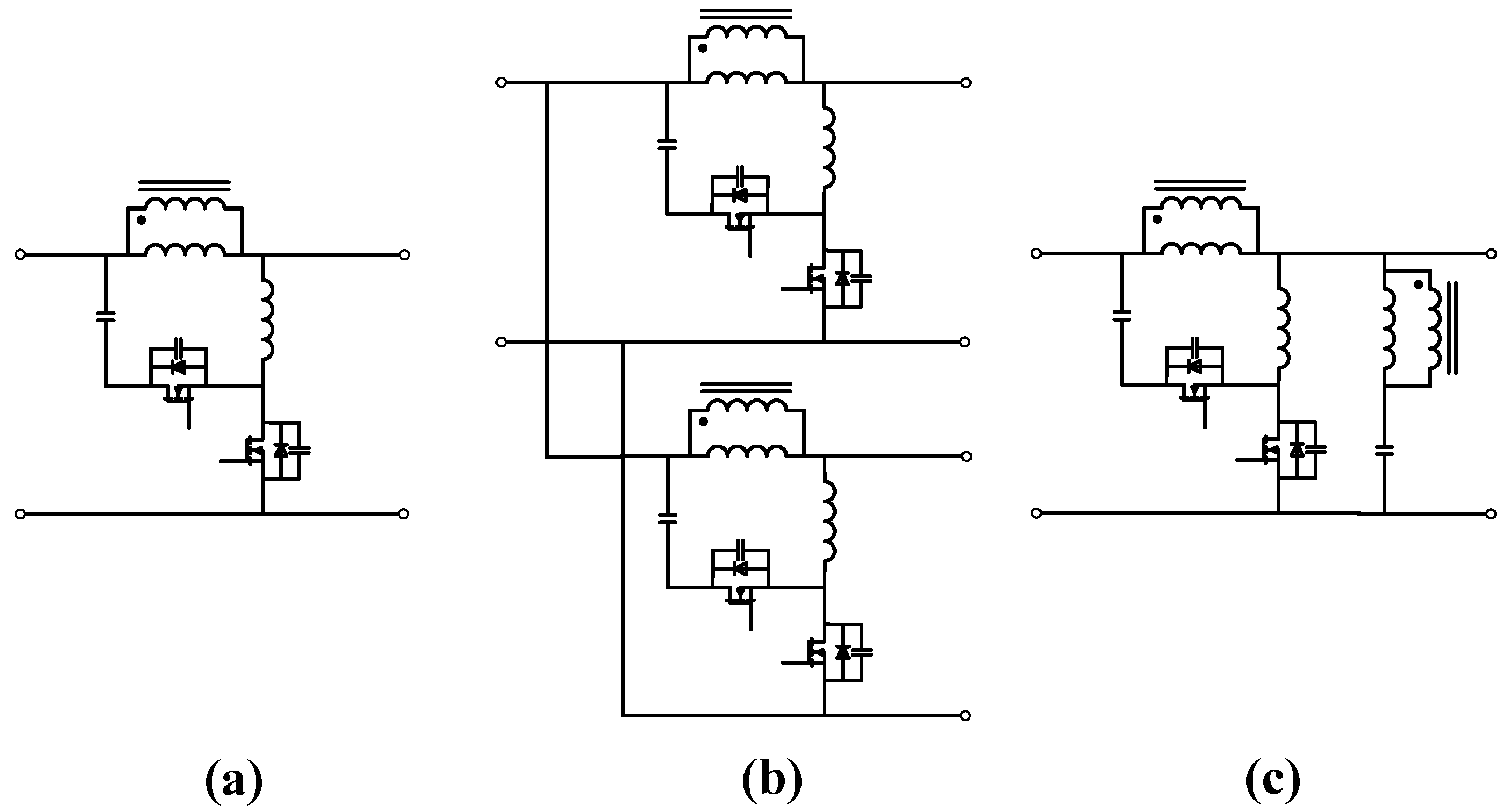
Figure 1 shows the basic coupled-inductor boost converter [14]. This boost converter uses the coupled inductor to replace the conventional inductor and utilizes the turn ratio to greatly increase the output voltage [15,16,17,18,19]. The basic coupled-inductor boost converter still has a critical disadvantage, where the leakage inductance of coupled inductor causes a high voltage spike when the power switch is turned off. Although increasing the turn ratio can increase the voltage gain, the leakage inductance is also increased. A lossless clamped circuit can reduce the voltage stress on the main switch as the circuit cannot realize ZVS of the main switch. The active clamp method utilizes resonance of the clamp capacitor and resonant inductor to recover energy. This method not only absorbs voltage spikes on power switches but also enables power switches to achieve ZVS [20,21,22]. Although increasing the duty cycle of power switch in the conventional coupled-inductor boost converter can achieve a higher voltage gain ratio, the power switch experiences a larger conduction loss due to the increase in turned-on time. Furthermore, the coupled inductor volume is larger than the inductor of the conventional boost converter because the coupled inductor has extra added due to the winding of the secondary side. Therefore, it is unsuitable for application in the solar microinverter. This method has a large DC current flows through the primary side of the coupled inductor. Finally, the passive components are increased, and the topology composition becomes more complex.
The cascaded coupled-inductor method is presented; this is different to the conventional boost converter [23,24]. This method can alleviate the voltage spike problem and recycle the leakage energy, but the clamping circuit causes extra losses. The stacked coupled inductor utilizes the flyback output directly to augment the boost output [25,26]. However an extra voltage balance control is required because the output terminal is divided into two capacitors. Similar to the stacked coupled inductor, a synchronous rectifier switch replaces the power diode in [27], allowing the main power switch to achieve ZVS, thereby improving conversion efficiency. Similar to the cascaded coupled-inductor method, the multi-winding coupled-inductor method uses additional windings to improve voltage gain and reduce power-diode voltage stress [28,29]. However, this approach increases passive component count and complicates the topology. The integrated coupled-inductor method [30,31,32] utilizes the characteristics of a boost or SEPIC converter to minimize input current ripple and reduce winding inductor core losses. This method exhibits higher topology complexity than the multi-winding coupled-inductor method and fails to achieve ZVS in the power switch. The above method has the problem of a large DC current flowing through the input inductor, and this problem remains unaddressed. The interleaved coupled-inductor method uses multiple converters operating in tandem to alleviate the current stress at the primary side of coupled inductors, but it does not increase the voltage gain [33,34]. Unfortunately, using multiple converter sets causes the circuit volume to increase and poses challenges in switch control for the interleaved method.
A dual-coupled-inductor-based high-step-up boost converter with active-clamping and zero-voltage switching is proposed. This method uses a stabilizing capacitor loop and dual coupled inductor, which is an innovative coupled-inductor converter and is different from existing inductor converter topology. The stabilizing capacitor voltage at stable conditions is equivalent to the input voltage; the energy of the dual coupled inductors is provided by the input voltage and stabilizing capacitor. The dual coupled inductors share the large input current at the primary side of coupled inductors and the secondary side of coupled inductors is connected in series to achieve high step-up voltage ratio. It extends the voltage gain dramatically and decreases the switch voltage stress. In addition, the active clamp method can transfer the energy released by the leakage inductance to the output load. Thus, the proposed topology can have more efficient performance.
Figure 2 shows that the primary side of the present topology is different from the basic coupled-inductor boost converter and interleaved method. Compared with basic coupled-inductor boost converters, the use of dual coupled inductors enables shared energy storage, allowing for the use of smaller magnetic components. Additionally, connecting the secondary sides of coupled inductors in series achieves a high step-up voltage ratio and the presented converter effectively reduces the duty cycle, thereby decreasing conduction losses in the main power switch because of reduced turn-on time. The proposed converter uses active clamping to suppress the voltage spikes and utilizes the leakage inductance of coupled inductors for ZVS operation in the power switches. Compared with the interleaved coupled-inductor converters and multiple coupled-inductor converters, it not only requires fewer circuit components but also features simpler switch control.
In Section 2, analyses of the circuit operations, operation waveform, and time domain are provided. In Section 3, analysis of circuit characteristics, component stress, and DC gain is outlined. This includes circuit design, which is discussed and calculated. In Section 4, testing of a prototype converter with 300 W output power, 25–40 VDC input voltage, and 200 VDC output voltage is described; the highest efficiency was around 94.7%.
2. Operation of the Proposed Converter
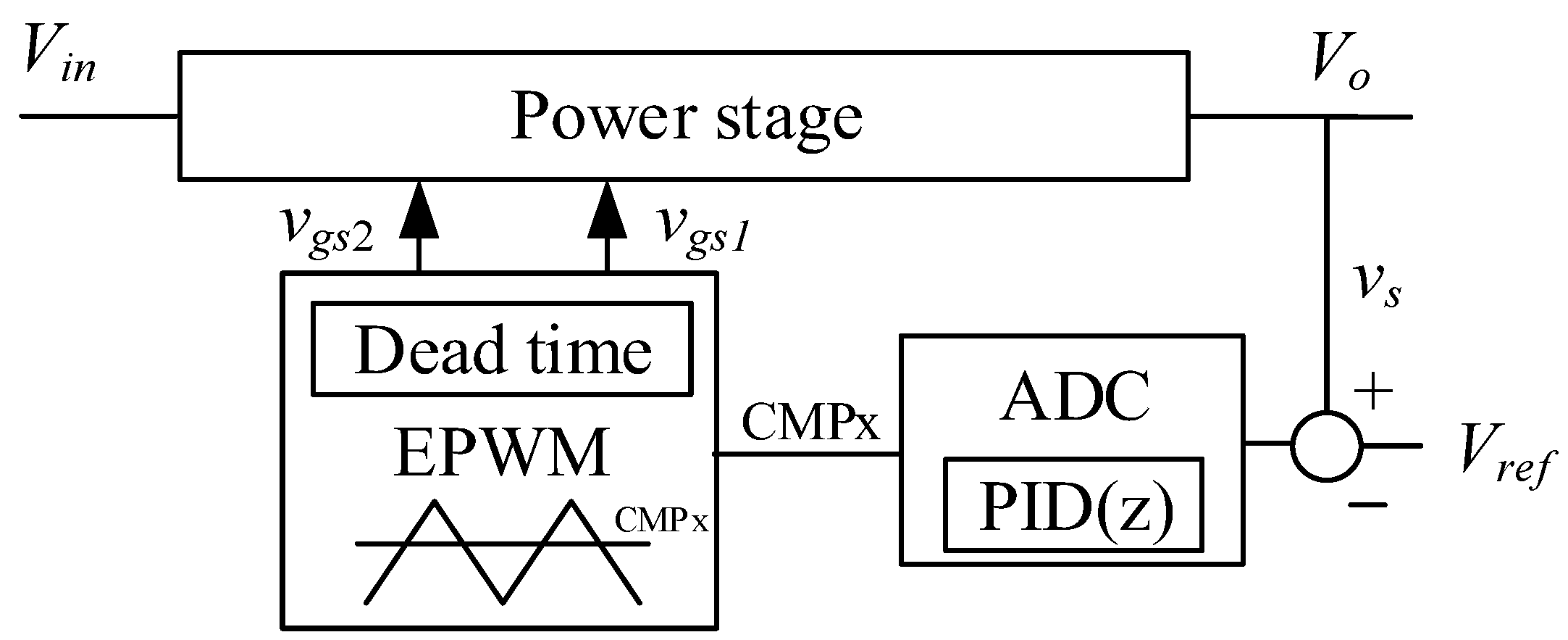
Figure 3 shows the schematic of the proposed boost converter using dual coupled inductors to achieve a high step-up ratio while implementing active clamping for ZVS. This topology comprises two identical coupled inductors CI1 and CI2, the main switch S1, the auxiliary switch S2, a resonant inductor Lr, a clamp capacitor Ca, a stabilizing capacitor Cb, and the output diode Do. Both coupled inductors share identical characteristics, and the ideal coupling coefficient is one. A transformer T model is used to describe the coupled inductors. The resonant inductor Lr was designed to enable ZVS for the S1 and S2 operations. The control method is pulse-width modulation (PWM). In this study, the vs signal is obtained by dividing the output voltage. The vs signal is compared with Vref, and the digital value is converted by the analog-to-digital converter (ADC) of the DSP. The CMPx value is derived after executing the proportional integral differential (PID) in the z-domain. Finally, intelligent EPWM generates the gate signal. PWM control maintains a fixed frequency while adjusting the pulse width to ensure a stable output voltage, as illustrated in Figure 4.
To analyze the proposed boost converter with dual coupled inductors and a high step-up ratio, the following assumptions are made:
- The turn ratio of the two coupled inductors is the same, which is 1:n.
- The magnetizing inductance of both coupled inductors is the same, which is Lm (Lm1 = Lm2 = Lm).
- The clamping capacitors Ca and Cb and the output capacitor Co are much larger than the output capacitance of power switches Cr1 and Cr2. Their steady-state voltages can be viewed as constant voltage sources, dependent on the input voltage and duty cycle.
- The on times of S1 and S2 are DTs and (1 − D)Ts, respectively, where D is the duty cycle of main switch S1, Ts is the switching period, and the dead time is assumed to be smaller than other conduction times.
- All components are considered ideal such that the conduction losses of all switches and diodes are ignored.
From the above assumptions, Ca and Cb in the steady state can be calculated. When the main switch S1 is turned on, the voltage across the primary side of CI1 approximates the input voltage Vin. On the contrary, when the main switch S1 is turned off, the voltage across the primary side of CI1 is approximately −vCa. From the flux balance of magnetizing inductance Lm under the steady state, vCa can be expressed as
The voltage across the primary side of CI2 approximates −vCb when S1 is turned on, and the voltage across the primary side of CI2 is Vin + vCa − vCb when main switch S1 is turned off. In accordance with Equation (1) and to maintain flux balance, the steady-state value of vCb can be determined as
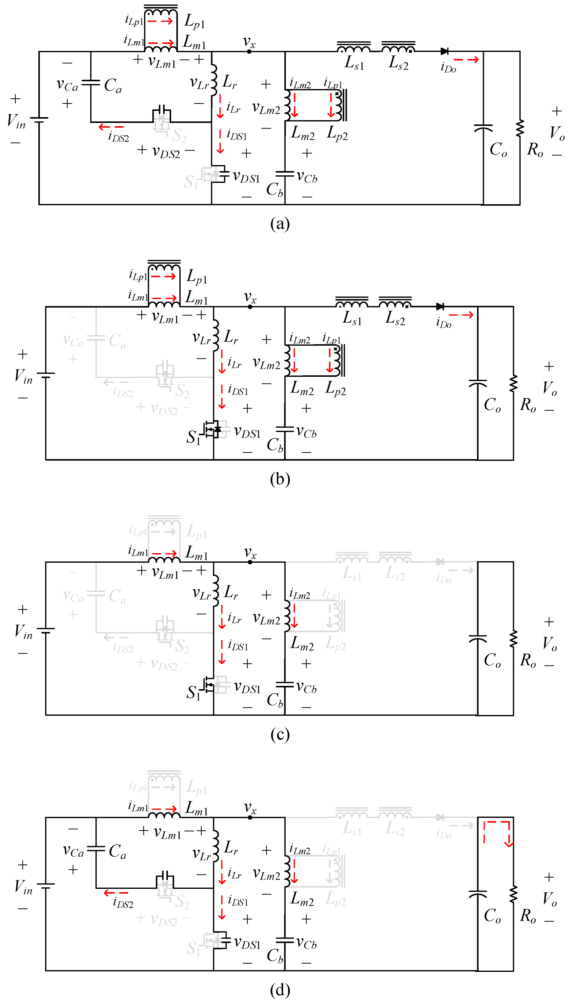
The definitions of the direction of voltage and current are shown in Figure 3. iDS1 and iDS2 are the currents of switches, iLr is the resonant inductor current, iLm1 and iLm2 are the magnetizing inductor currents, iLp1 and iLp2 are the currents of coupled inductors at the primary side, and iDo is the output diode current. Figure 5 shows the operation waveform of the proposed topology. The waveform can be divided into six parts in one cycle. The descriptions of each state are given below. Figure 6 provides a visual representation of these six operation states.
- -
- State 1 (t0–t1)
In this state, auxiliary switch S2 is turned off at t0, whereas the main switch S1 remains off. The resonant inductor Lr has two parasitic capacitors Cr1 and Cr2, and the direction of resonant inductor current iLr is negative. This state ends when capacitor Cr1 is discharged to zero and capacitor Cr2 is charged to Vin + vCa. The values of Cr1 and Cr2 are extremely small, so this state is extremely short. The resonant inductor Lr must meet the following conditions to achieve ZVS:
- -
- State 2 (t1–t2)
At t1, Cr1 is discharged to zero, the body diode operates across S1, and S1 is turned on to achieve ZVS. At the same time, both coupled inductors still provide energy to the output side, and the output diode current iDo continually decreases linearly until it reaches zero. iLr changes from negative to positive until it is equal to the sum of absolute value of magnetizing inductor currents iLm1 and iLm2, and this stage ends. The node voltage vx and the magnetizing inductor voltages vLm1 and vLm2 can be expressed as
The magnetizing inductor currents iLm1(t) and iLm2(t), resonant inductor current iLr(t), and diode current iDo(t) can be expressed as
- -
- State 3 (t2–t3)
In state 3, S1 remains on and carries the resonant inductor current iLr, and iLr is equal to the sum of the absolute value of magnetizing inductor currents iLm1 and iLm2. S2 is remains off, vLm1 is approximately equal to the input voltage Vin, and vLm2 is approximately equal to the negative input voltage −Vin, so the input energy is shared between the two primary magnetizing inductances of coupled inductor. This interval ends when S1 is turned off. The output diode is reverse biased, and the output current is supplied only by the output capacitor Co. The node voltage vx and the magnetizing inductor voltages vLm1 and vLm2 can be expressed as
The magnetizing inductor currents iLm1(t) and iLm2(t) and resonant inductor current iLr(t) can be expressed as
- -
- State 4 (t3–t4)
At t3, S1 and S2 are turned off. The resonant inductor Lr is resonant with parasitic capacitors Cr1 and Cr2. This stage ends when capacitor Cr1 is charged to Vin + vCa and capacitor Cr2 is discharged to zero. This stage is extremely short because the values of capacitances Cr1 and Cr2 are extremely small. The ZVS condition is expressed as
- -
- State 5 (t4–t5)
Figure 6e shows the operation station at this state, where the voltage vDS1 is to be charged to Vin + vCa. The resonant inductor current iLr flows through the body diode of S2, and S2 is turned on to achieve ZVS. Given that vLm1 is approximately equal to the negative vCa and vLm2 is approximately equal to vCa, the output diode Do is forward biased and starts to operate. The energies stored in the magnetizing inductors Lm1 and Lm2 are transferred to the output load. The diode current iDo starts to increase linearly, and clamp capacitor voltage vCa begins to rise. This stage ends when the resonant inductor current iLr decreases to zero. The node voltage vx and the magnetizing inductor voltages vLm1 and vLm2 can be expressed as
The currents iLm1, iLm2, iLr, and iDo are given as
- -
- State 6 (t5–t6)
The circuit operations in this interval are the same as those in State 5, except for the directions of iLr. The capacitor voltage vCa starts to decrease, and the ampere-second balance is completed in States 5 and 6.
3. Analysis of the Proposed Converter
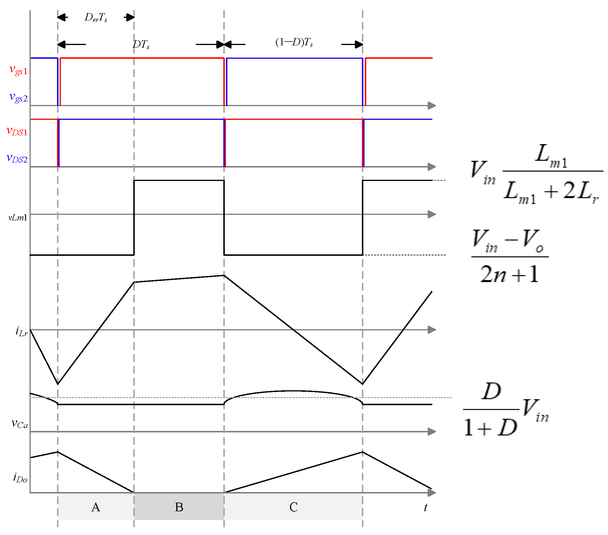
Figure 7 ignores the intervals t0–t1 and t3–t4 of Figure 3. The intervals t0–t1 and t3–t4 can be ignored because the time is extremely short. Simplifications are needed to derive the ideal transfer function of the proposed topology. Figure 5 shows the simplified waveform, where D is the duty cycle of metal–oxide–semiconductor field-effect transistor (MOSFET) S1, and Der is the duty loss. The resonant inductor current iLr can be divided into stages A, B, and C, in accordance with its shape.
3.1. Clamped Voltage vCa
As shown in Equation (1), vCa is determined by D and Vin. As depicted in Figure 8, the clamp capacitor voltage vCa will be higher than the input voltage Vin if duty cycle D is higher than 0.5. If duty cycle D is close to 1, then the clamp capacitor voltage vCa will be extremely high. Therefore, in applications, the duty cycle should be designed around 0.5.
3.2. Voltage Transfer Ratio
In accordance with the simplified waveform at Figure 6, the volt-second balance equation of magnetizing inductor Lm1 is
In general, resonant inductor Lr is smaller than magnetizing inductors Lm1 and Lm2. If the effects of duty loss Der and resonant inductor Lr are ignored, then Equation (25) can be simplified as Equation (26), and ideal transfer function Mideal is derived as Equation (27).
Figure 9 shows the comparison of ideal transfer ratio Mideal and conventional boost converter transfer ratio M = 1/(1 − D). The proposed topology has a relatively higher transfer ratio. The transfer gain increases relatively because the transformer turn ratio is higher. In accordance with Equation (27), if the transfer ratio is around 10 times, then the turn ratio n = 1 is unsuitable.
Figure 10 shows the transfer ratio comparison of the proposed topology and coupled-inductor boost converter, where the transfer ratio of the proposed topology is (nD + 1)/(1 − D). From Figure 10, the transfer ratio of the proposed topology is higher than coupled-inductor boost converter when the turn ratio is the same.
The voltage of the magnetizing inductor Lm1 is inconsistent in duty cycle D due to the influence of duty loss Der. The effect of the inductor is also reconsidered, so Equation (28) is rederived, and the transfer ratio M = Vo/Vin can be expressed as
Equation (25) is used to derive duty loss Der as follows:
where iDo_Max is the peak current of diode, and the value can be derived as
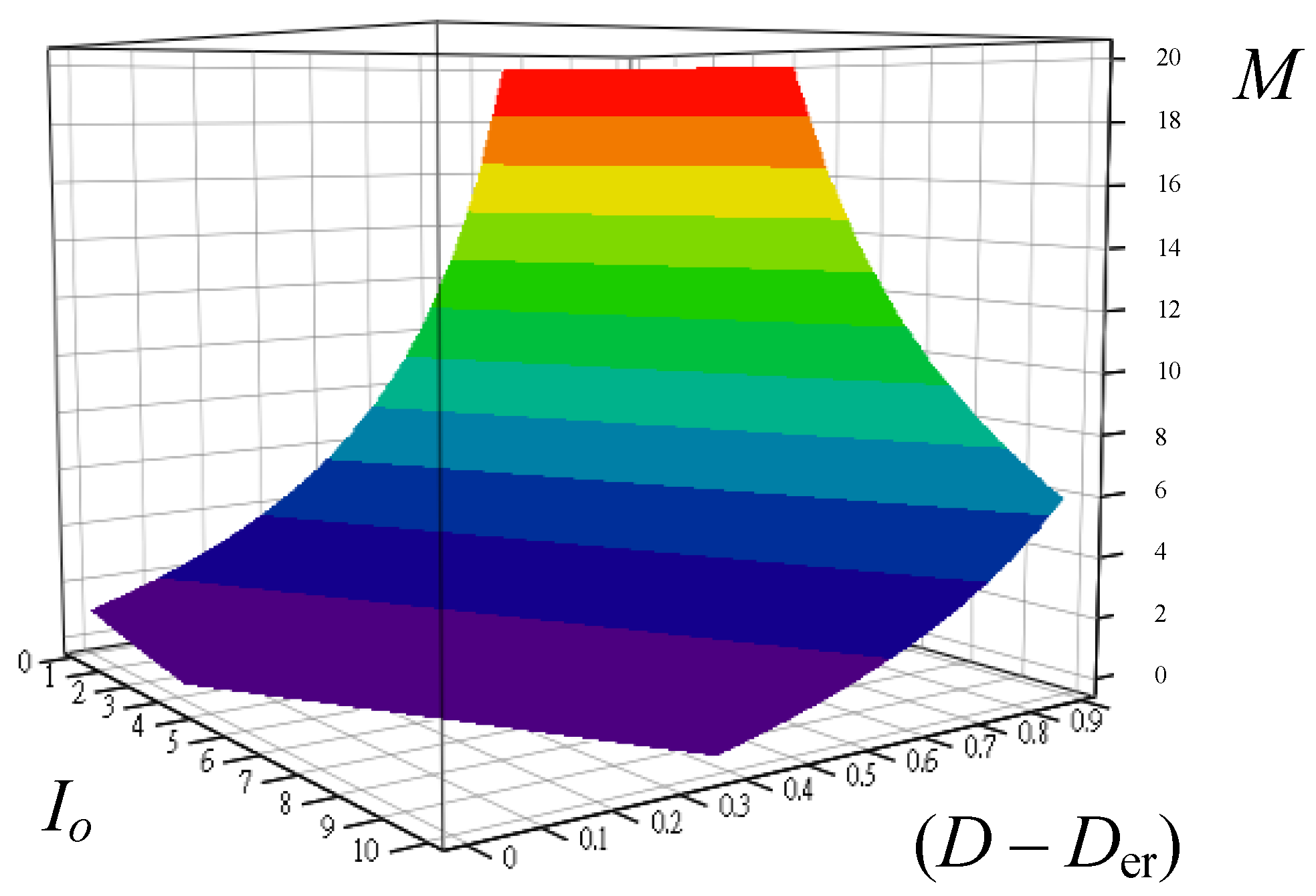
Figure 11 shows the relationship between transfer ratio M, output current Io, and duty cycle D, plotted using Equations (28)–(31). The transfer ratio M is affected by output current Io and duty cycle D. Duty loss Der increases with the increase in load current, which indicates that more duty cycle D is required to reach the required voltage. Assuming that the transfer ratio M is 8, duty cycle D changes from 0.52 to 0.69 if the output current Io changes from 0 to 3.
3.3. Voltage and Current Stress
In accordance with Section 2, the voltage stresses of switches S1 and S2, and diode Do can be derived as Equations (32) and (33). Resonant inductor Lr is smaller than magnetizing inductors Lm1 and Lm2, so voltage stress vDo can be simplified to facilitate subsequent comparison.
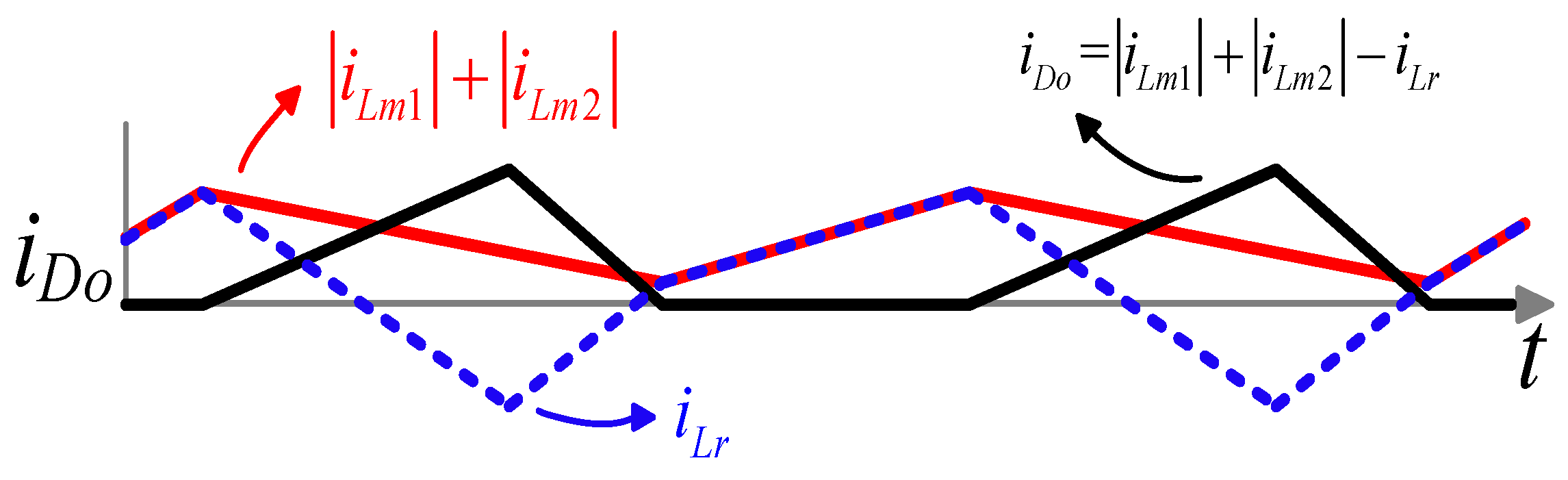
Figure 12 shows the relationship of magnetizing inductor currents iLm1 and iLm2, diode current iDo, and output current Io. From Equation (30), the value of output current Io is the average of diode current iDo. From Section 2, the diode current iDo is composed of magnetizing inductor currents iLm1 and iLm2 and resonant inductor current iLr. Two transformers provide current to the output, so the current stress of the transformer is lower.
Table 1 compares the modern topology and the proposed topology, which includes the number of components, voltage gain, control method, input current stress, diode voltage stress, and efficiency. Comparison is made under the same output load and current ripple conditions and the same output load conditions. The cascade coupled-inductor method increases the number of turns. As a result, the winding area of the magnetic components is increased, requiring the use of larger iron cores. Therefore, the voltage stress on the output diode also increases [21]. The stacked coupled inductor approach requires redundant rectifier diodes to control the output capacitor voltage [26]. Similar to stacked coupled inductors, the multi-winding coupled inductor approach uses additional windings to increase the voltage gain. The additional windings require magnetic components to be designed using larger cores [29]. However, the approach of stacked and multi-winding increases passive component count and complicates the topology. In the above method, the problem of a large DC current flowing through the input inductor remains unaddressed. The interleaved coupled-inductor method uses multiple converters operating in tandem to alleviate the current stress at the primary side of the coupled inductors [34]. Unfortunately, using multiple converter sets causes the circuit volume to increase and poses challenges in switch control for the interleaved method. Compared with previous studies, the primary side of the coupled inductor has a lower current stress under the same output load conditions. Considering the high output transfer ratio condition, the voltage stress of the proposed topology is around Vin, and the voltage stress of the conventional boost converter is higher than Vin.
4. Experimental Results
A 300 W prototype was designed and built to verify the feasibility of the proposed topology, as shown in Figure 13. The dimensions were approximately . The specifications of the prototype are shown in Table 2, and the selection of components is shown in Table 3. In addition, to verify the assumptions in Section 2, the parameters are listed in Table 4.
The inductance of resonant inductor was designed in accordance with Equations (3) and (29). The magnetizing inductance was based on Equations (12), (19) and (29). The parasitic capacitor was the output capacitance of MOSFET. Efficiency data were obtained from the experimental results. The DC power source utilized was the Keysight E35234A, the DC load was the Chroma 63108A, and the power meter was the HIOKI PW3337.
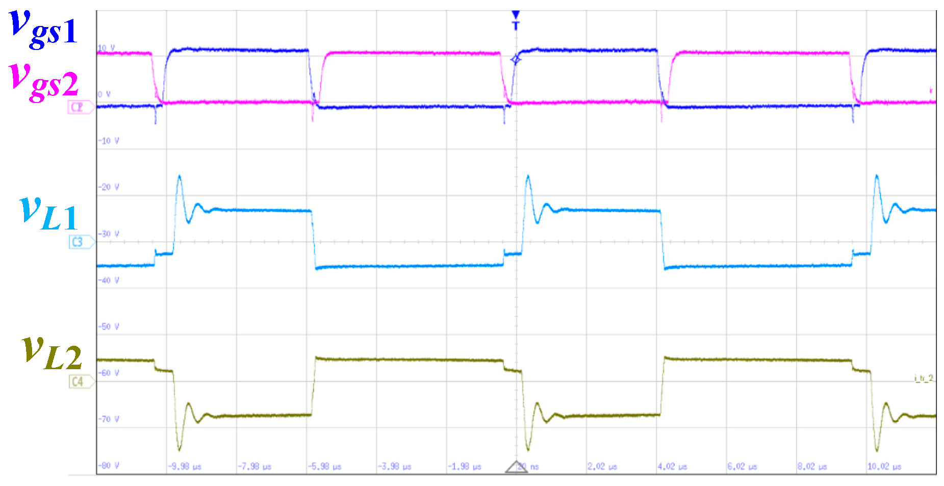
Figure 14, Figure 15 and Figure 16 show the operation waveforms at 25 V Vin and full load condition. The voltage stress of vDS2 mostly conformed to Equation (31). The voltage stress of vDS1 was slightly higher than the calculation because the capacitance vCa was small (this phenomenon can be referred to as State C in Figure 5). Figure 14 illustrates the ZVS waveforms. Before vgs1 and vgs2 were turned on, the drain-to-source voltages vDS1 and vDS2 were clamped at zero. Therefore, ZVS operations for S1 and S2 were achieved. Figure 15 and Figure 16 show the current waveform of resonant inductor iLr, diode iDo, and two switches iDS2 and iDS2.
Figure 17 illustrates the waveforms of the gate signals, vgs1 and vgs2, and the couple inductors voltage, vLm1 and vLm2 at 40 V Vin and full load condition. Both vLm1 and vLm2 had the identical voltage level through one complete switching cycle, and the operating condition was at 40 V Vin and full-load.
Figure 18 shows the waveforms of the gate-to-source vgs1, the secondary side’s voltage of the coupled inductors vLS1 and vLS2, and the current of the output diode iDo at 40 V Vin and full load condition. vLS1 and vLS2, had the identical voltage level through the one complete switching cycle, and when the output diode Do was to be forward-bias, the output current iDo was flowing through the secondary side of the coupled inductors LS1 and LS2 This meant that the dual coupled inductors provided energy to output capacitor Co and load.
Figure 19 and Figure 20 show the voltage levels of capacitors Ca and Ca at 25 V Vin, 40 V Vin, and 100% load. The average voltage value of vCa was approximately 53.3 V, which is similar to the result of Equation (1).
Figure 21 shows the efficiency curves at 25 V and 40 V Vin. The highest efficiency point was at 40 V Vin under 40% load.
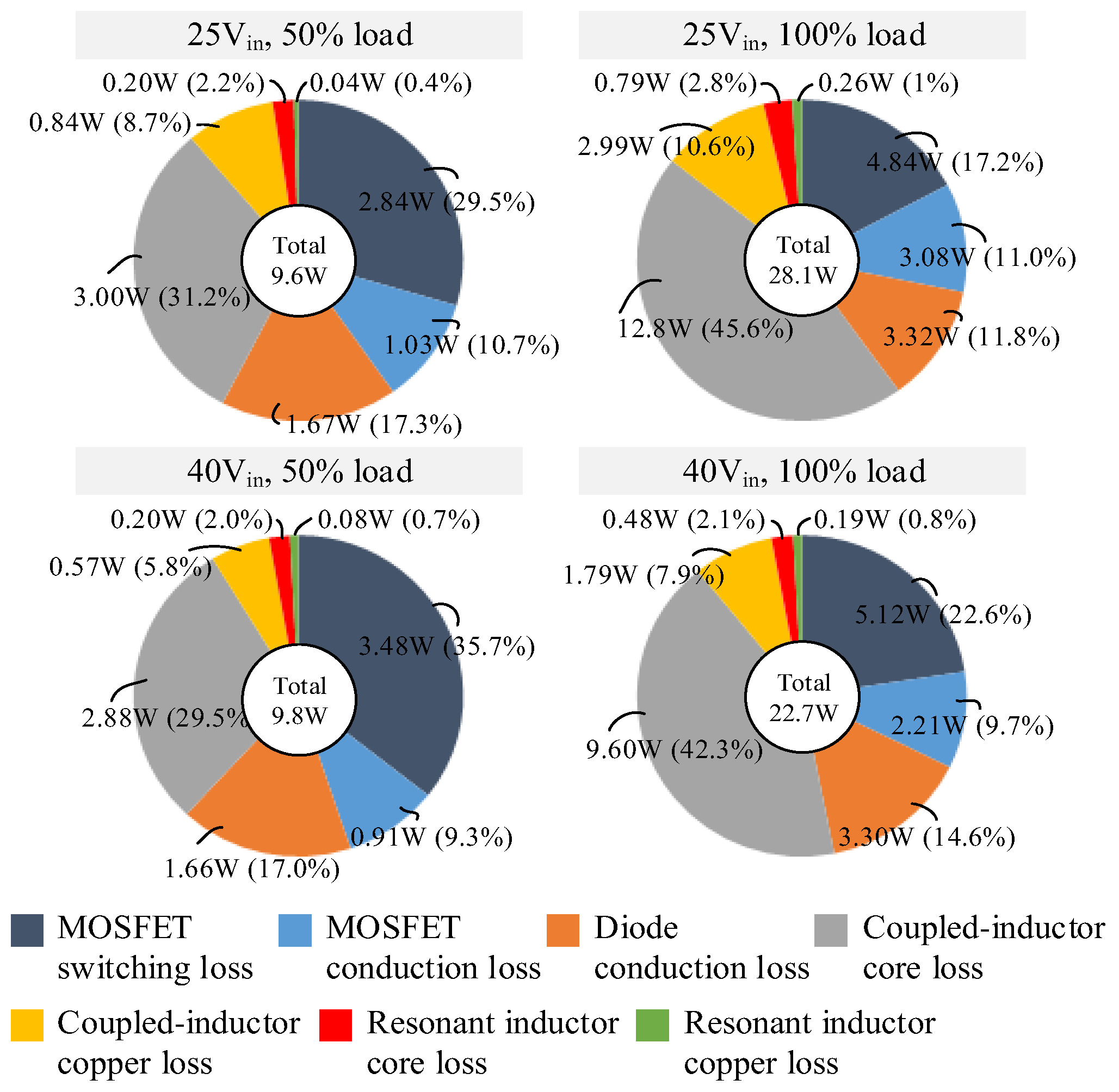
The loss analysis is obtained by recording the stress of the components experimentally and bringing it into the loss Equation (34). PS_sw is the switching loss of the main switch S1 and the auxiliary switch S2. PS_con is the conduction loss of the main switch S1 and the auxiliary switch S2. PD_con is the conduction loss of the output diode. PTr_core is the core loss of the two coupled inductors. PTr_core is the core loss of the two coupled inductors. PLr_core is the core loss of the resonant inductor. PLr_core is the core loss of the resonant inductor. The loss obtained by the component parameters and the stress equations was consistent with the actual efficiency. Figure 22 shows the loss distribution at 50% and 100% loads. The highest power loss was the coupled inductor core loss. Although the two switches reached ZVS, the turn-off loss remained high and was the second highest power loss.
5. Conclusions
This study introduces an innovative high-step-up boost converter design featuring two separate coupled inductors. This approach enables the creation of a low-profile implementation, with the secondary side of coupled inductors connected in series to increase the step-up voltage ratio. An active clamp is also incorporated to achieve ZVS, making it particularly well-suited for the design of low-profile solar microinverters. Operating modes throughout a complete switching cycle are described, and key equations are derived. The experimental results on a 300 W, input voltage 25–40 V, and output voltage 200 V prototype are recorded to verify the theoretical analysis. The maximum efficiency was around 94.7%. The proposed converter not only facilitates low-profile designs but also meets the stringent requirements of high step-up voltage ratios.
Author Contributions
Software, C.-T.C.; Validation, C.-T.C.; Writing—original draft, S.-H.C.; Writing—review & editing, Y.-F.L. All authors have read and agreed to the published version of the manuscript.
Funding
This research received no external funding.
Data Availability Statement
The original contributions presented in the study are included in the article, further inquiries can be directed to the corresponding author.
Conflicts of Interest
The authors declare no conflict of interest.
References
- Aghdam, F.H.; Abapour, M. Reliability and cost analysis of multistage boost converters connected to PV panels. IEEE J. Photovolt. 2016, 6, 981–989. [Google Scholar] [CrossRef]
- Agorreta, J.L.; Reinaldos, L.; Gonzalez, R.; Borrega, M.; Balda, J.; Marroyo, L. Fuzzy switching technique applied to PWM boost converter operating in mixed conduction mode for PV systems. IEEE Trans. Ind. Electron. 2009, 56, 4363–4373. [Google Scholar] [CrossRef]
- Liu, J.; Wang, K.; Zheng, Z.; Li, C.; Li, Y. A dual-active-clamp quasi-resonant isolated boost converter for PV integration to medium-voltage DC grids. IEEE J. Emerg. Sel. Top. Power Electron. 2019, 8, 3444–3456. [Google Scholar] [CrossRef]
- Ma, G.; Qu, W.; Yu, G.; Liu, Y.; Liang, N.; Li, W. A zero-voltage-switching bidirectional dc–dc converter with state analysis and soft-switching-oriented design consideration. IEEE Trans. Ind. Electron. 2009, 56, 2174–2184. [Google Scholar]
- Ma, K.W.; Lee, Y.S. A novel uninterruptible dc-dc converter for UPS applications. IEEE Trans. Ind. Appl. 1992, 28, 808–815. [Google Scholar] [CrossRef]
- Kovatchev, E.; Evstatieva, N. Design of a digitally controlled boost converter for automotive headlamp applications. In Proceedings of the 2017 International Scientific Conference Electronics (ET), Sozopol, Bulgaria, 13–15 September 2017; pp. 1–4. [Google Scholar]
- Gacio, D.; Calleja, A.J.; García, J.; Ribas, J.; Rico-Secades, M. Suitable switching converter topologies for automotive signal lamps and headlamps using power LEDs. In Proceedings of the 2008 IEEE Industry Applications Society Annual Meeting, Edmonton, AB, Canada, 5–9 October 2008; pp. 1–7. [Google Scholar]
- Sreeja, P.; Suresh, L.P. Optimized design of ZVZCS switched non isolated DC-DC boost converter with high voltage gain. In Proceedings of the 2013 International Conference on Circuits, Power and Computing Technologies (ICCPCT), Nagercoil, India, 20–21 March 2013; pp. 500–505. [Google Scholar]
- Barbi, I.; Gules, R. Isolated DC-DC converters with high-output voltage for TWTA telecommunication satellite applications. IEEE Trans. Power Electron. 2003, 18, 975–984. [Google Scholar] [CrossRef]
- Kiran, R.; Kalpana, R. Design and development of modular dual-input DC/DC step down converter for telecom power supply. In Proceedings of the 2018 IEEE International Conference on Power Electronics, Drives and Energy Systems (PEDES), Chennai, India, 18–21 December 2018; pp. 1–6. [Google Scholar]
- Akerlund, J. -48 V DC computer equipment topology-an emerging technology. In Proceedings of the INTELEC-Twentieth International Telecommunications Energy Conference (Cat. No. 98CH36263), San Francisco, CA, USA, 4–8 October 1998; pp. 15–21. [Google Scholar]
- Tofoli, F.L.; Pereira, D.D.C.; de Paula, W.J.; de Sousa Oliveira Júnior, D. Survey on non-isolated high-voltage step-up dc–dc topologies based on the boost converter. IET Power Electron. 2015, 8, 2044–2057. [Google Scholar] [CrossRef]
- Gu, Y.; Zhang, D.; Zhao, Z. Input/output current ripple cancellation and RHP zero elimination in a boost converter using an integrated magnetic technique. IEEE Trans. Power Electron 2015, 30, 747–756. [Google Scholar] [CrossRef]
- Vazquez, N.; Estrada, L.; Hernandez, C.; Rodriguez, E. The tapped-inductor boost converter. In Proceedings of the 2007 IEEE International Symposium on Industrial Electronics, Vigo, Spain, 4–7 June 2007; pp. 538–543. [Google Scholar]
- Ai, J.; Lin, M. Ultra large gain step-up coupled-inductor DC-DC converter with an asymmetric voltage multiplier network for a sustainable energy system. IEEE Trans. Power Electron 2017, 31, 6896–6903. [Google Scholar] [CrossRef]
- Tintu, V.R.; George, M. Tapped inductor technology based DC-DC converter. In Proceedings of the 2011 International Conference on Signal Processing, Communication, Computing and Networking Technologies, Thuckalay, India, 21–22 July 2011; pp. 747–753. [Google Scholar]
- Lee, J.J.; Cho, B.H. A novel high step-up zero-current-switching tapped-inductor boost converter. In Proceedings of the 8th International Conference on Power Electronics-ECCE Asia, Jeju, Republic of Korea, 30 May–3 June 2011; pp. 1869–1872. [Google Scholar]
- Berkovich, Y.; Axelrod, B. Switched-coupled inductor cell for DC–DC converters with very large conversion ratio. IET Power Electron. 2011, 4, 309–315. [Google Scholar] [CrossRef]
- Li, W.; He, X. Review of non-isolated high-step-up DC/DC converters in photovoltaic grid-connected applications. IEEE Trans. Ind. Electron. 2010, 58, 1239–1250. [Google Scholar] [CrossRef]
- Duarte, C.M.C.; Barbi, I. A Family of ZVS-PWM Active-Clamping DC-to-DC Converters: Synthesis, Analysis, Design, and Experimentation. IEEE Trans. Circuits Syst. I Fundam. Theory Appl. 1997, 44, 698–704. [Google Scholar] [CrossRef]
- Zhao, Y.; Li, W.; He, X. Single-phase improved active clamp coupled inductor-based converter with extended voltage doubler cell. IEEE Trans. Power Electron. 2012, 27, 2869–2878. [Google Scholar] [CrossRef]
- Hwz, K.I.; Yau, Y.T. High step-up converter based on coupling inductor and bootstrap capacitors with active clamping. IEEE Trans. Power Electron. 2014, 29, 2655–2660. [Google Scholar]
- Zhao, Q.; Lee, F.C. High-efficiency, high step-up DC-DC converters. IEEE Trans. Power Electron. 2003, 18, 65–73. [Google Scholar] [CrossRef]
- Van de Sype, D.M.; De Gusseme, K.; Renders, B.; Van den Bossche, A.R.; Melkebeek, J.A. A single switch boost converter with a high conversion ratio. In Proceedings of the Twentieth Annual IEEE Applied Power Electronics Conference and Exposition, 2005. APEC 2005, Austin, TX, USA, 6–10 March 2005; pp. 1581–1587. [Google Scholar]
- Hsieh, Y.P.; Chen, J.F.; Liang, T.J.; Yang, L.S. Novel high step-up DC–DC converter with coupled-inductor and switched-capacitor techniques. IEEE Trans. Ind. Electron. 2011, 59, 998–1007. [Google Scholar] [CrossRef]
- Liang, T.J.; Chen, S.M.; Yang, L.S.; Chen, J.F.; Ioinovici, A. Ultra-large gain step-up switched-capacitor DC-DC converter with coupled inductor for alternative sources of energy. IEEE Trans. Circuits Syst. I Regul. Pap. 2012, 59, 864–874. [Google Scholar] [CrossRef]
- Spiazzi, G.; Mattavelli, P.; Costabeber, A. Effect of parasitic components in the integrated boost-flyback high step-up converter. In Proceedings of the 2009 35th Annual Conference of IEEE Industrial Electronics, Porto, Portugal, 3–5 November 2009; pp. 420–425. [Google Scholar]
- Wai, R.J.; Lin, C.Y.; Duan, R.Y.; Chang, Y.R. High-efficiency DC-DC converter with high voltage gain and reduced switch stress. IEEE Trans. Ind. Electron. 2007, 54, 354–364. [Google Scholar] [CrossRef]
- Tseng, K.C.; Lin, J.T.; Huang, C.C. High step-up converter with three-winding coupled inductor for fuel cell energy source applications. IEEE Trans. Power Electron. 2014, 30, 574–581. [Google Scholar] [CrossRef]
- Hu, X.; Gong, C. A high voltage gain DC–DC converter integrating coupled-inductor and diode–capacitor techniques. IEEE Trans. Power Electron. 2013, 29, 789–800. [Google Scholar]
- Deng, Y.; Rong, Q.; Li, W.; Zhao, Y.; Shi, J.; He, X. Single-switch high step-up converters with built-in transformer voltage multiplier cell. IEEE Trans. Power Electron. 2012, 27, 3557–3567. [Google Scholar] [CrossRef]
- Chen, S.M.; Liang, T.J.; Yang, L.S.; Chen, J.F. A cascaded high step-up DC–DC converter with single switch for microsource applications. IEEE Trans. Power Electron. 2010, 26, 1146–1153. [Google Scholar] [CrossRef]
- Dwari, S.; Parsa, L. An efficient high-step-up interleaved DC–DC converter with a common active clamp. IEEE Trans. Power Electron. 2010, 26, 66–78. [Google Scholar] [CrossRef]
- Li, W.; Zhao, Y.; Deng, Y.; He, X. Interleaved converter with voltage multiplier cell for high step-up and high-efficiency conversion. IEEE Trans. Power Electron. 2010, 25, 2397–2408. [Google Scholar] [CrossRef]
Figure 1.
Conventional coupled-inductor boost converter.

Figure 2.
Primary side of coupled-inductor boost converters includes (a) basic, (b) interleaved, and (c) stabilizing capacitor loops.
Figure 2.
Primary side of coupled-inductor boost converters includes (a) basic, (b) interleaved, and (c) stabilizing capacitor loops.

Figure 3.
Schematic of the proposed boost converter using dual coupled inductors to achieve high step-up ratio with active clamping for ZVS.
Figure 3.
Schematic of the proposed boost converter using dual coupled inductors to achieve high step-up ratio with active clamping for ZVS.

Figure 4.
Control mode of the proposed high step-up ratio boost converter.

Figure 5.
Key waveforms of the proposed high step-up ratio boost converter with ZVS.

Figure 6.
Conduction paths of (a) State 1, (b) State 2, (c) State 3, (d) State 4, (e) State 5, and (f) State 6 for the proposed boost converter with high step-up ratio and ZVS during one switching period.
Figure 6.
Conduction paths of (a) State 1, (b) State 2, (c) State 3, (d) State 4, (e) State 5, and (f) State 6 for the proposed boost converter with high step-up ratio and ZVS during one switching period.


Figure 7.
Simplified waveform.

Figure 8.
Voltage stress of clamp capacitor vCa.

Figure 9.
Transfer ratio comparison of the proposed topology and conventional boost converter.

Figure 10.
Transfer ratio comparison of the proposed topology and conventional coupled-inductor boost converter.
Figure 10.
Transfer ratio comparison of the proposed topology and conventional coupled-inductor boost converter.

Figure 11.
Output transfer ratio.

Figure 12.
Relationship of magnetizing inductor, diode, and output currents.

Figure 13.
Prototype of the proposed topology.

Figure 14.
Operation waveforms of vgs1, vgs2, vDS1, and vDS2 at 100% load. (Time: 2 µs/div; vgs1: 10 V/div; vgs2: 10 V/div; vDS1: 50 V/div; vDS2: 50 V/div).
Figure 14.
Operation waveforms of vgs1, vgs2, vDS1, and vDS2 at 100% load. (Time: 2 µs/div; vgs1: 10 V/div; vgs2: 10 V/div; vDS1: 50 V/div; vDS2: 50 V/div).

Figure 15.
Operation waveforms of vgs1, vgs2, iDS1, and iDS2 at 100% load. (Time: 2 µs/div; vgs1: 10 V/div; vgs2: 10 V/div; iDS1: 20 A/div; iDS2: 20 A/div).
Figure 15.
Operation waveforms of vgs1, vgs2, iDS1, and iDS2 at 100% load. (Time: 2 µs/div; vgs1: 10 V/div; vgs2: 10 V/div; iDS1: 20 A/div; iDS2: 20 A/div).

Figure 16.
Operation waveforms of vgs1, vgs2, iLr, and iDo at 100% load. (Time: 2 µs/div; vgs1: 10 V/div; vgs2: 10 V/div; iLr: 20 A/div; iDo: 5 A/div).
Figure 16.
Operation waveforms of vgs1, vgs2, iLr, and iDo at 100% load. (Time: 2 µs/div; vgs1: 10 V/div; vgs2: 10 V/div; iLr: 20 A/div; iDo: 5 A/div).

Figure 17.
Operation waveforms of vgs1, vgs2, vL1, and vL2 at 100% load. (Time: 2 µs/div; vgs1: 10 V/div; vgs2: 10 V/div; vL1: 50 V/div; vL2: 50 A/div).
Figure 17.
Operation waveforms of vgs1, vgs2, vL1, and vL2 at 100% load. (Time: 2 µs/div; vgs1: 10 V/div; vgs2: 10 V/div; vL1: 50 V/div; vL2: 50 A/div).

Figure 18.
Operation waveforms of vgs1, vLS1, vLS2 and iDo at 100% load. (Time: 2 µs/div; vgs1: 10 V/div; vLS1: 200 V/div; vLS2: 200 V/div; iDo: 5 A/div).
Figure 18.
Operation waveforms of vgs1, vLS1, vLS2 and iDo at 100% load. (Time: 2 µs/div; vgs1: 10 V/div; vLS1: 200 V/div; vLS2: 200 V/div; iDo: 5 A/div).

Figure 19.
Voltage levels of capacitors Ca and Cb at 25 V Vin, 100% load. (Time: 2 µs/div; vgs1: 10 V/div; vgs2: 10 V/div; vCa: 20 V/div; vCb: 20 V/div).
Figure 19.
Voltage levels of capacitors Ca and Cb at 25 V Vin, 100% load. (Time: 2 µs/div; vgs1: 10 V/div; vgs2: 10 V/div; vCa: 20 V/div; vCb: 20 V/div).

Figure 20.
Voltage levels of capacitors and at 40 V Vin, 100% load. (Time: 2 µs/div; : 10 V/div; : 10 V/div; vCa: 20 V/div; vCb: 20 V/div).
Figure 20.
Voltage levels of capacitors and at 40 V Vin, 100% load. (Time: 2 µs/div; : 10 V/div; : 10 V/div; vCa: 20 V/div; vCb: 20 V/div).

Figure 21.
Efficiency curve.

Figure 22.
Loss distribution.


Table 1.
Comparison of the conventional boost converter and the proposed topology.
| Topologies | Propose Converter | [21] | [26] | [29] | [34] |
|---|---|---|---|---|---|
| Number of coupled inductors | 2 | 1 | 1 | 1 | 2 |
| Number of switches | 2 | 2 | 2 | 1 | 2 |
| Number of diodes | 1 | 2 | 4 | 4 | 4 |
| Voltage gain | |||||
| Control method | PWM | PWM | PWM | PWM | Interleave |
| Soft-switching performance | ZVS | ZVS | Hard switching | Hard switching | Hard switching |
| Input-current stress | Medium | High | High | High | Medium |
| Diode-voltage stress | High | High | Low | Low | Medium |
| Conduction losses | Low | High | High | High | High |
Table 2.
Specification of Prototype.
| Item | Value |
|---|---|
| 25–40 V | |
| 200 V | |
| 1.5 A | |
| 300 W | |
| 100 kHz |
Table 3.
Component Selection.
| Item | Value |
|---|---|
| FDP2614 | |
| BYC200-600P | |
| Transformer turn ratio | 1:3 |
| Core material/type | PC 40/PQ35-35 |
Table 4.
Parameters of Components.
| Item | Value |
|---|---|
| Resonant inductor Lr | 1 μH |
| Magnetizing inductance Lm | 15 μH |
| Parasitic capacitor Cr | 500 pF |
| Voltage-stable capacitor Ca | 66 μF |
| Clamping capacitor Cb | 8 μF |
Disclaimer/Publisher’s Note: The statements, opinions and data contained in all publications are solely those of the individual author(s) and contributor(s) and not of MDPI and/or the editor(s). MDPI and/or the editor(s) disclaim responsibility for any injury to people or property resulting from any ideas, methods, instructions or products referred to in the content. |
© 2024 by the authors. Licensee MDPI, Basel, Switzerland. This article is an open access article distributed under the terms and conditions of the Creative Commons Attribution (CC BY) license (https://creativecommons.org/licenses/by/4.0/).
Share and Cite
MDPI and ACS Style
Chen, S.-H.; Chen, C.-T.; Lin, Y.-F. Dual-Coupled-Inductor-Based High-Step-Up Boost Converter with Active-Clamping and Zero-Voltage Switching. Energies 2024, 17, 2018. https://0-doi-org.brum.beds.ac.uk/10.3390/en17092018
AMA Style
Chen S-H, Chen C-T, Lin Y-F. Dual-Coupled-Inductor-Based High-Step-Up Boost Converter with Active-Clamping and Zero-Voltage Switching. Energies. 2024; 17(9):2018. https://0-doi-org.brum.beds.ac.uk/10.3390/en17092018
Chicago/Turabian StyleChen, Sheng-Hua, Chuan-Ting Chen, and Yi-Feng Lin. 2024. "Dual-Coupled-Inductor-Based High-Step-Up Boost Converter with Active-Clamping and Zero-Voltage Switching" Energies 17, no. 9: 2018. https://0-doi-org.brum.beds.ac.uk/10.3390/en17092018
Note that from the first issue of 2016, this journal uses article numbers instead of page numbers. See further details here.